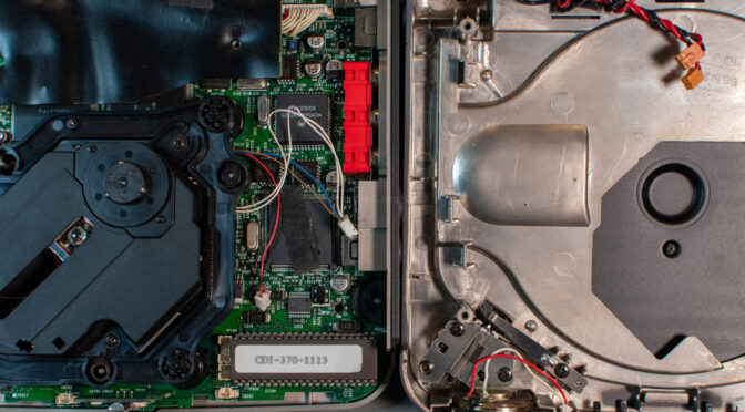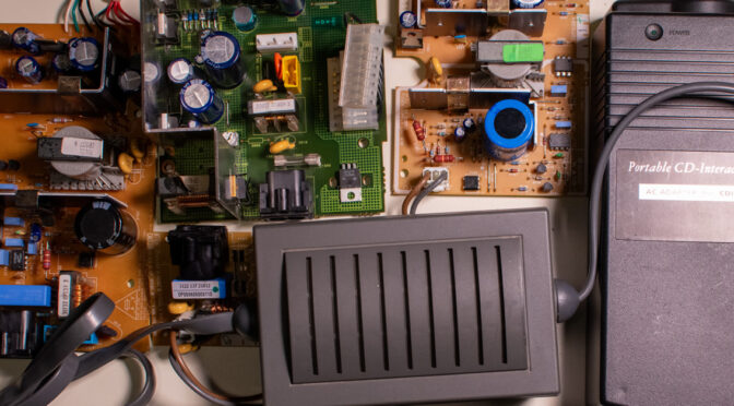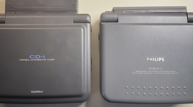
This GoldStar GPI-1200M is an earlier version of the Philips CDI 370 shown here. Internally, both systems appear to share almost identical hardware and were manufactured by LG. The most obvious differences are the external case design, system ROM and user interface.
Defects: Input ports 1 and 2 are non-functional. As a result, no input devices can be used and diagnostic functions such as Service Shell or low-level tests cannot be accessed. The original battery pack is no longer functional. This hardware is also known for failures of several tantalum capacitors.
- Resources
- Player shell
- Service Shell
- System ROM
- Disassembly, PCBs and markings (body)
- Disassembly top case and lid
- Disassembly, PCBs and markings (display)
- GIA-110 (power supply unit)
- To-Do
- History
Resources
- Service manual: N/A
- GoldStar / LG (portable players)
- GoldStar / LG Electronics CD-i players
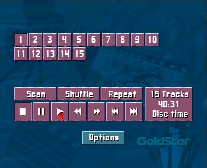
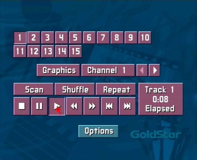
Player shell
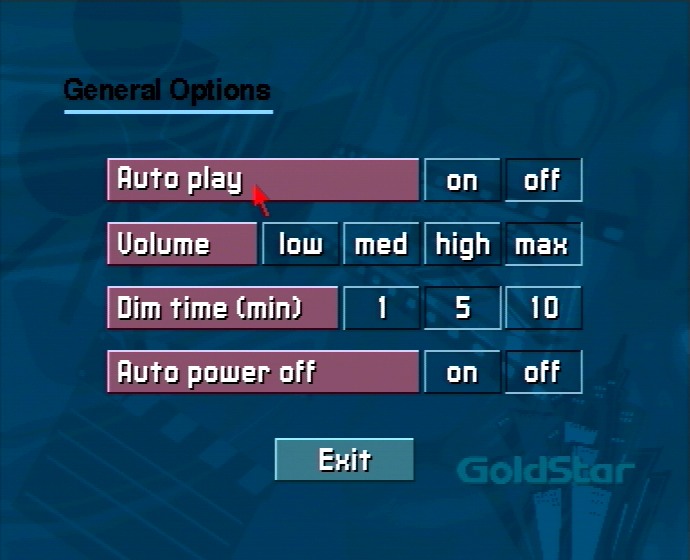
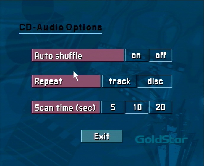
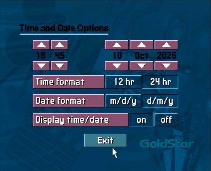
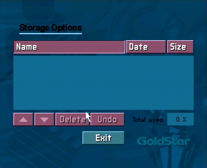
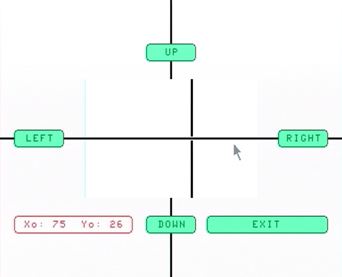
Service Shell
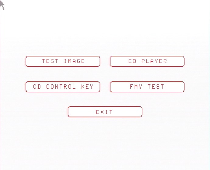
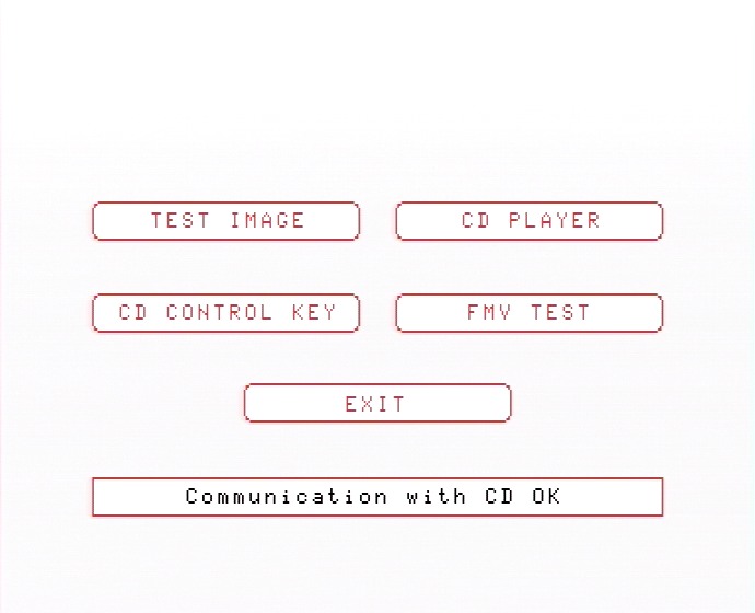
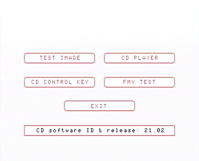
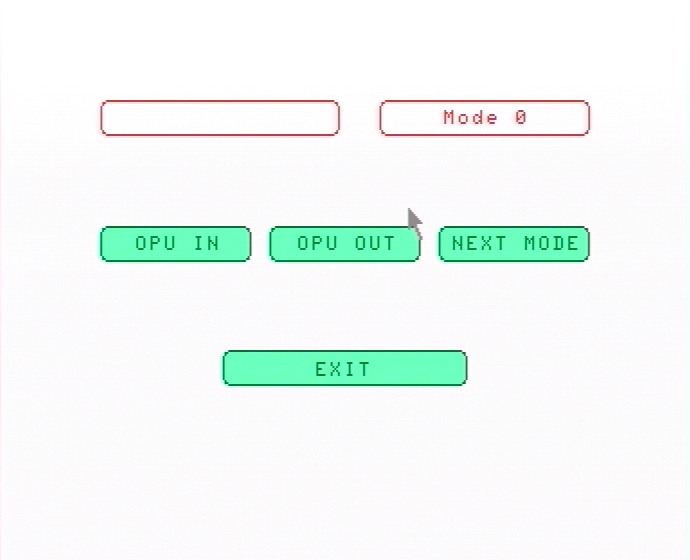
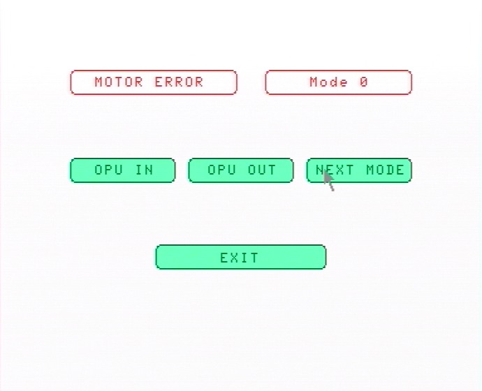
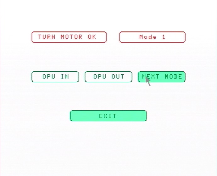
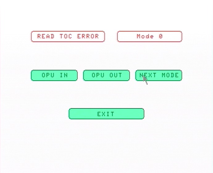
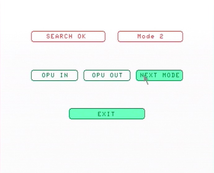
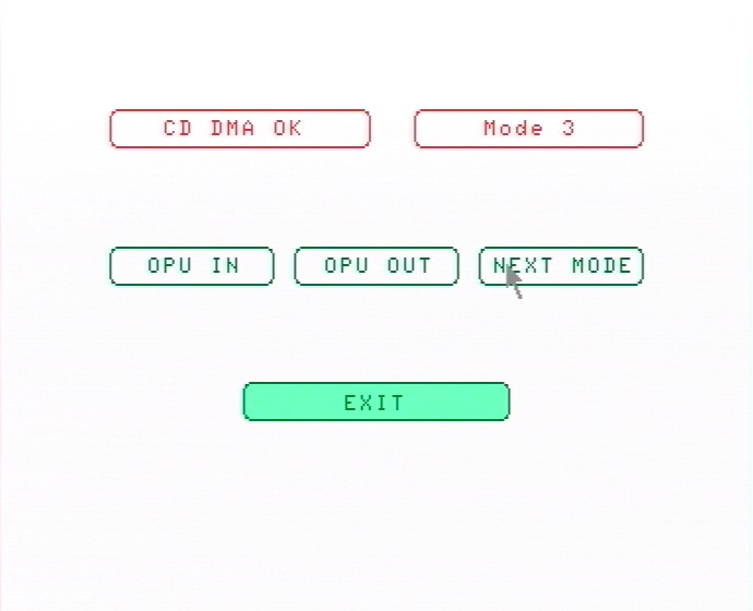
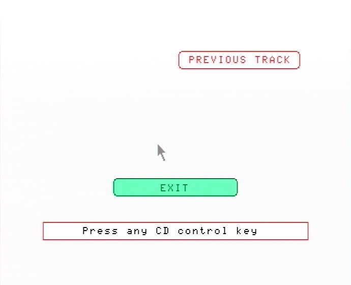
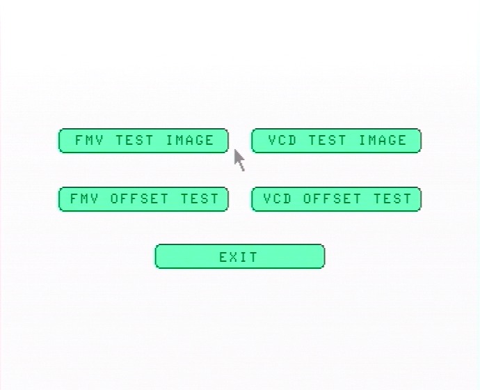
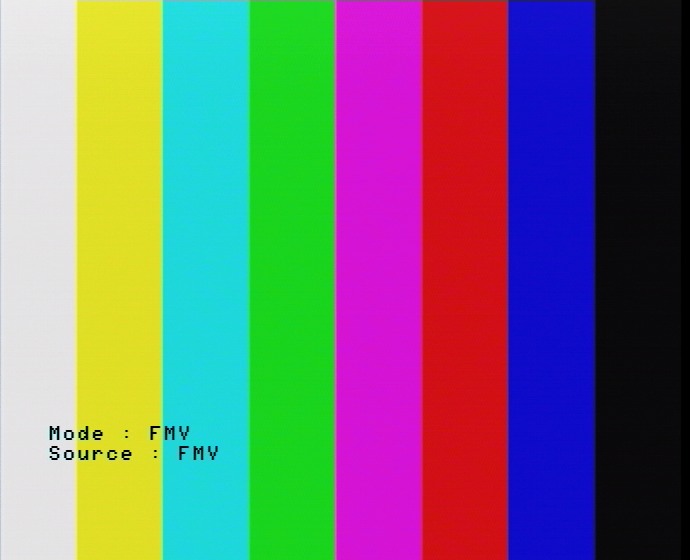
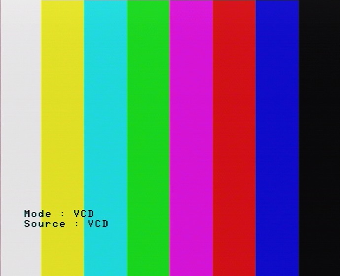
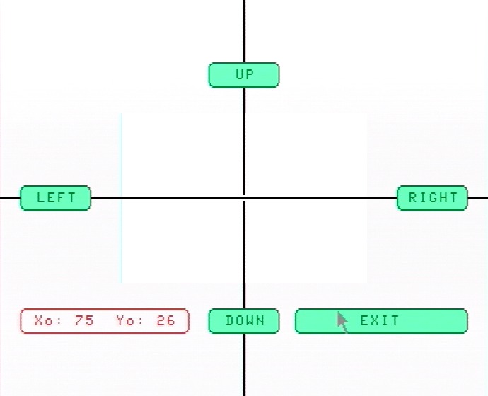
You can launch the Service Shell, as with most other Philips CD-i players, by shorting pins 2 and 3 on INPUT 1. (Search for “Service Shell” on this website to find further examples, such as this one).
Please note that you cannot acces the Service Shell if a controller is connected to INPUT 2.
Important: The lid switch is bypassed in the Service Shell. This means that the laser remains active even when the lid is open, and the turntable motor will also activate as soon as a disc is detected.

System ROM
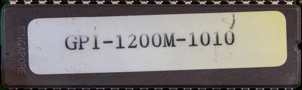
The system ROM ID 10 R1.0 is stored in a Texas Instruments TMS 27C240-15 262144 by 16-bit EPROM.
Low-level test:
                Portable CD-I Low Level Test    Rel. 1.0
                ============================    ========

                Press any key to test receiver
                Receiver o.k., you pressed:   20

                Initializing VDSC registers...

        0. Exit Low Level test
        1. Writing to a default RAM address
        2. ROM parity check
        3. NVRAM test (32K)
        4. DRAM test
        5. FMV/FMA test
        6. CD/AP Interface test
        7. Chip Select test
        8. VDSC test


        Make your Selection: 2


-         ROM ID: 10
- Release Number: 10
-       CheckSum: 0000EE9E
Modules and checksums:
  Addr     Size      Owner    Perm Type Revs  Ed #  Crc   Module name
-------- -------- ----------- ---- ---- ---- ----- ------ ------------
000054d0    27562     0.0     0555 Sys  a000    83 eed568 kernel
0000c07a      390     0.0     0555 Sys  8000    22 3733e3 init
0000c200     4830     0.0     0555 Sys  a000    29 6aabc9 csdinit
0000d4de      256     0.0     0777 5    8001     1 18c03f csd_pcdi
0000d5de      572     0.0     0555 Sys  a000     7 7a0b0e tk340_pcdi
0000d81a      886     0.0     0555 Subr 8020     1 55eed9 rtclock
0000db90      460     0.0     0555 Prog 80f0     8 a4ec9f sysgo
0000dd5c     6318     0.0     0555 Prog 8001     7 898c3d config
0000f60a     6130     0.0     0555 Prog 8001     7 eb0353 dvconf
00010dfc     4510     0.0     0555 Fman a003    96 a4d145 cdfm
00011f9a    15002     0.254   0555 Driv a004    99 7ec739 cddrv
00015a34      128     0.0     0555 Desc 8000     1 860f4f ap
00015ab4      128     0.0     0555 Desc 8000     1 a85bde cd
00015b34     5592     0.0     0555 Fman a000    17 63023d nrf
0001710c       94     0.0     0555 Desc 8000     1 b525ad nvr
0001716a      774     0.0     0555 Driv a001     6 81a3e9 nvdrv
00017470     1930     0.0     0555 Fman a000    29 56fcb0 scf
00017bfa     1990     0.0     0555 Driv a000    16 c00f59 sc68340
000183c0      124     0.0     0555 Desc 8000     6 26ae2d term
0001843c      122     0.0     0555 Desc 8000     6 c0ea77 t1
000184b6      122     0.0     0555 Desc 8000     6 4c453f t2
00018530     2848     0.0     0555 Fman a00b    35 28611f ucm
00019050    66722     0.0     0555 Driv a011    50 f77db6 video
000294f2      130     0.0     0555 Desc 8000     1 2cd0ab vid
00029574      130     0.0     0555 Desc 8000     1 e92acb vd2
000295f6      134     0.0     0555 Desc 8000     1 bf3638 vdk
0002967c      134     0.0     0555 Desc 8000     1 d9575a vk1
00029702      134     0.0     0555 Desc 8000     1 d94389 vk2
00029788     2526     0.0     0555 Driv a001    26 257f09 mspcdi
0002a166      136     0.0     0555 Desc 8000     1 273401 ptr
0002a1ee      136     0.0     0555 Desc 8000     1 e58305 pt2
0002a276     2478     0.0     0555 Driv a001     1 2c22ba pckpcdi
0002ac24      132     0.0     0555 Desc 8000     1 dee86f newkids
0002aca8     2104     0.0     0555 Driv a001     1 a26282 kbdriv
0002b4e0      130     0.0     0555 Desc 8000     1 0ec068 kbd
0002b562      130     0.0     0555 Desc 8000     1 990ff4 kb2
0002b5e4     2270     0.0     0555 Fman a000    35 d6a976 pipeman
0002bec2      118     0.0     0555 Desc 8000     2 f0652e nil
0002bf38      172     0.0     0555 Driv a000     1 407f81 null
0002bfe4      102     0.0     0555 Desc 8000     2 cf450e pipe
0002c04a     7762     0.0     0555 Fman a000     0 6166e0 MoviMan
0002de9c    13142     0.0     0555 Driv a00f    15 ea5e22 fmvdrv
000311f2     8514     0.0     0555 Driv a000     5 d2dde9 madriv
00033334      122     0.0     0555 Desc 8000     1 240767 mv
000333ae      104     0.0     0555 Desc 8000     1 7d738a ma
00033416    16512     0.0     0333 Data 8001     1 ce3755 dspcode
00037496     3840     0.0     0333 Data 8001     1 a9bd1e vmpeg
00038396     7798     1.0     0555 Trap c001    13 46c5dc math
0003a20c    18082    10.48    0555 Trap c00a     6 5f673d cio
0003e8ae     2992     0.0     0555 Data 8020     1 191a59 FONT8X8
0003f45e    42796     0.0     0555 Prog 8001    17 3a6122 vs
00049b8a    28000     0.0     0555 Prog 8001     2 d323a5 options
000508ea     4876     0.0     0555 Prog 8001     7 bf9a7c discheck
00051bf6     1962     0.253   0555 Prog 8002     7 6d3736 vcd
000523a0     2816     0.0     0555 Prog 8001     7 603427 launcher
00052ea0     6510     0.0     0777 Data 8000     1 5391a8 font3.ft
0005480e     3932     1.0     0777 Data 8002     1 cd32be upslbd11.ai1
0005576a     3200     0.0     0777 Data 8001     1 c32bc4 cdaudio5.img
000563ea     7360     0.0     0777 Data 8001     1 2e833f cddapla5.img
000580aa     3712     0.0     0777 Data 8001     1 f9986a general5.img
00058f2a     2784     0.0     0777 Data 8001     1 fca7fa gslogo.img
00059a0a     4944     0.0     0777 Data 8001     1 a01900 logo.img
0005ad5a    50704     0.0     0777 Data 8001     1 22b107 main.img
0006736a     2000     0.0     0777 Data 8001     1 e9a9b6 options5.img
00067b3a     3664     0.0     0777 Data 8001     1 b4bc02 storage5.img
0006898a     4352     0.0     0777 Data 8001     1 103037 timedat5.img
00069a8a      560     0.0     0777 Data 8001     1 5cb348 cdaudio5.clt
00069cba      560     0.0     0777 Data 8001     1 2894fc cddapla5.clt
00069eea      560     0.0     0777 Data 8001     1 69372c general5.clt
0006a11a      560     0.0     0777 Data 8001     1 2672c6 gslogo.clt
0006a34a      560     0.0     0777 Data 8001     1 c59269 logo.clt
0006a57a      560     0.0     0777 Data 8001     1 73e1ec main.clt
0006a7aa      560     0.0     0777 Data 8001     1 fdc9a0 mainb.clt
0006a9da      560     0.0     0777 Data 8001     1 ee8566 options5.clt
0006ac0a      560     0.0     0777 Data 8001     1 cd9995 storage5.clt
0006ae3a      560     0.0     0777 Data 8001     1 9a68d5 timedat5.clt
0006b06a    20856     0.0     0555 Prog 8001     2 132388 service
000701e2    20836     1.0     0555 Prog c001    53 f7cb17 shell

    File             Addr    Size    Type             Description
------------------ -------- ------ ------------------ ------------
gpi1200m10.rom 00000000   512K gpi1200m10.rom     GoldStar GPI-1200M system ROM 1.0
gpi1200m10.rom 00000000   512K gpi1200m.mdl       GoldStar GPI-1200M player
gpi1200m10.rom 00000000   512K goldstar.brd       Goldstar board
gpi1200m10.rom 00000000   512K pmpeg.dvc          Portable CD-i digital video
gpi1200m10.rom 00000000   512K gpi1200m10.tag     {512K} ID: 10 Rel: 10 Sum: EE9E
gpi1200m10.rom 00000000   512K gpi1200m10.crc     CRC: D0A4E36D
gpi1200m10.rom 00000000   512K gpi1200m10.md5     MD5: 2A8B8235C1EE9DA0756A5776208A9D87
Disassembly, PCBs and markings (body)
To disassemble the body, remove the marked screws on the bottom and rear of the unit.
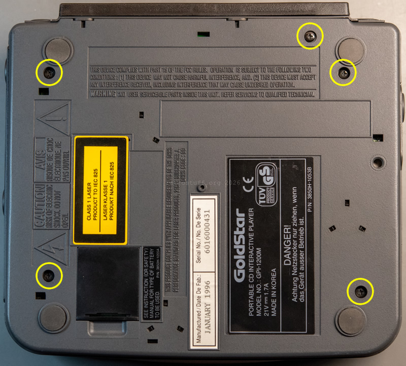
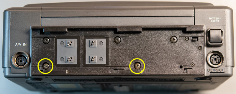
Turn the unit over and carefully lift the front half of the housing. Disconnect the speaker cables before opening it completely.
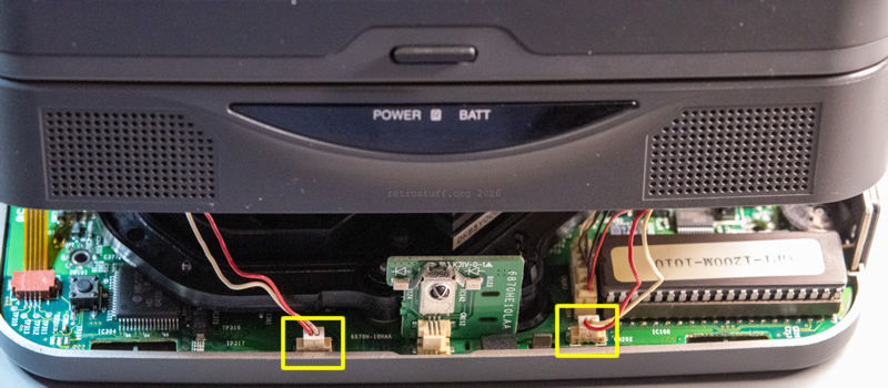
Disconnect the connectors marked with rectangles:
- FFC to the controls (do not pull the cable out immediately. First release the connector lock by lifting it slightly, then remove the FFC).
- Two connectors leading to the battery contacts.
- Display connector.
The top cover and display assembly can now be set aside in a safe location.
The cover of the power PCB can be removed after removing the two marked screws.
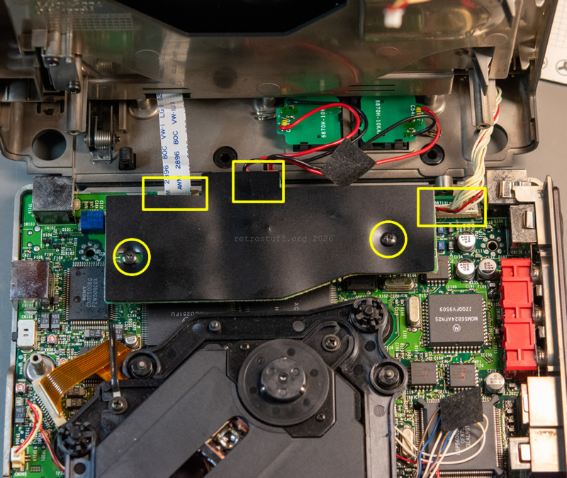
This provides a good view of the power and battery charging PCB. The board can now simply be lifted out. Do not place it too far away, as it is required to power up the unit during testing. It is also recommended to keep the IR PCB nearby if you intend to control the player using an RC6 22ER9055 CD-i Commander.
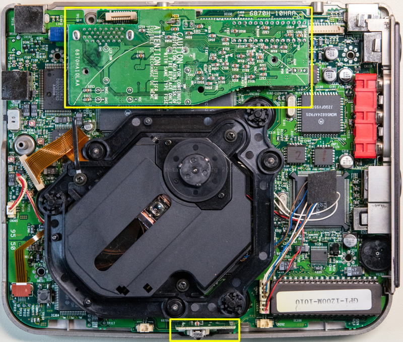
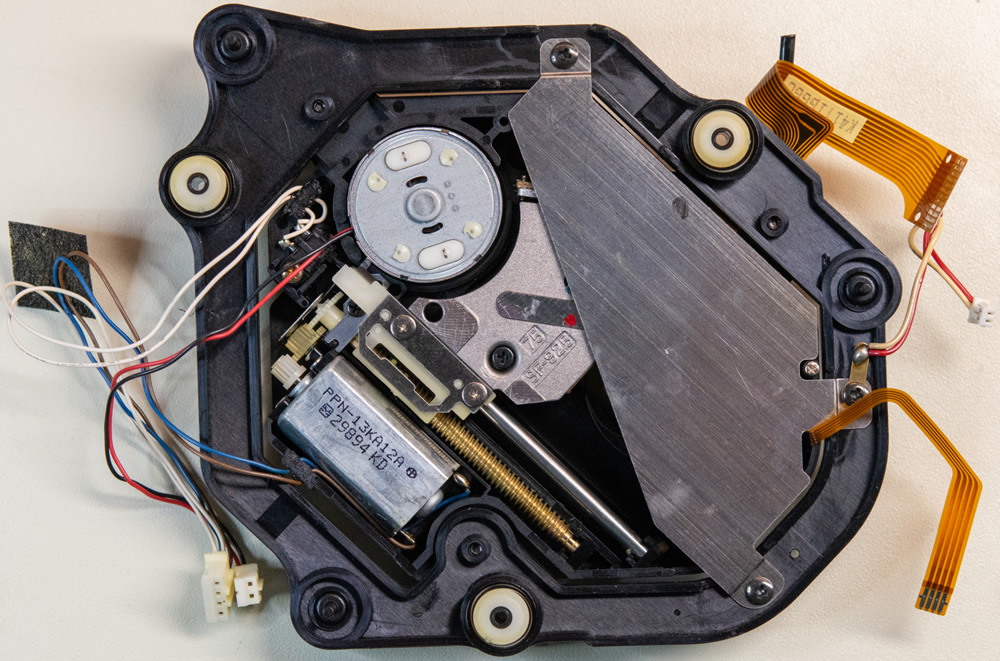
Next is the CD mechanism. This is the most delicate part of the disassembly procedure, so pay close attention.
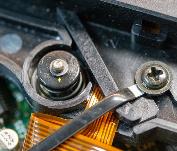
The mechanism is supported by three rubber sockets located in the bottom case (underneath the orange circles) and three guide shafts with spring-loaded cylinders (yellow circles). Do not simply pull the mechanism out and do not attempt to remove the cylinders from the shafts, as reassembly can be difficult.
First, disconnect the five connectors marked by yellow rectangles. The upper FFC must be unlocked before removal, while the lower FFC can be pulled out directly.
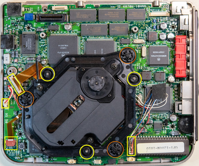
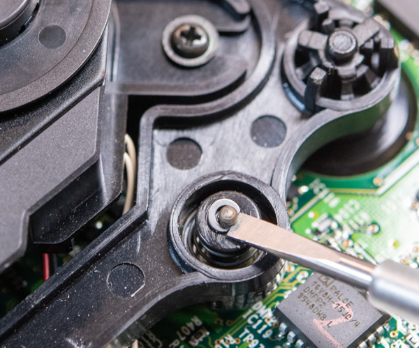
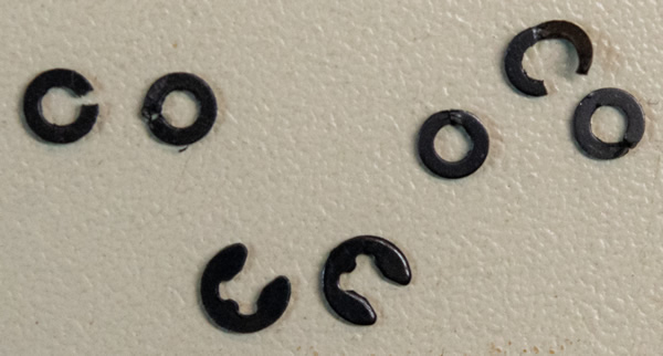
Next, locate the three circlips that retain the spring-loaded cylinders. The opening in each circlip is difficult to see, but it is present (see arrow). Using a small flat-blade screwdriver, push towards the opening to slide the circlip off the shaft.
In case of loss or damage, they can be replaced with standard 1,5 mm circlips commonly found in inexpensive assortment kits.
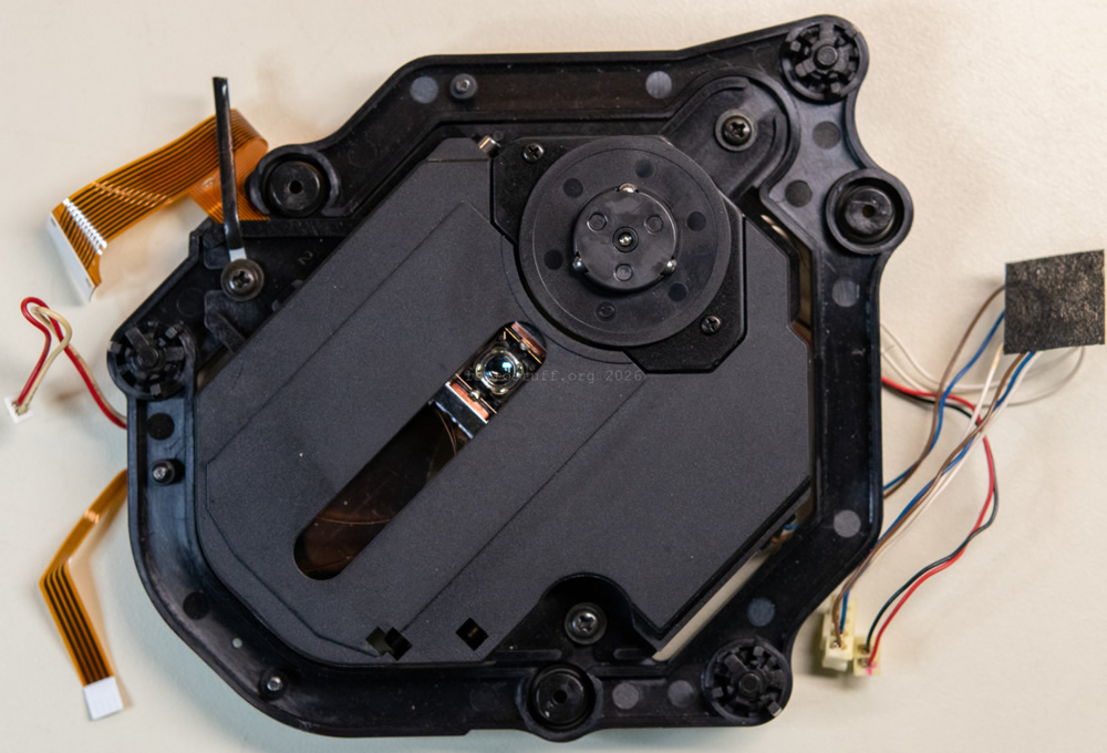
The CD mechanism can now be separated from the mainboard and lower case by lifting it straight upwards.
If one or more cylinders remain stuck on the shafts, do not apply force. Instead, carefully assist them with a flat-blade screwdriver by levering them upwards at the rim. The mechanism should come free without significant force.
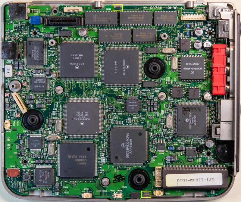
To remove the mainboard from the bottom case, pull back the two marked plastic retaining clips.
Do not apply unnecessary force, as the clips can break easily. The plastic bezel on the left side of the mainboard can then be removed.
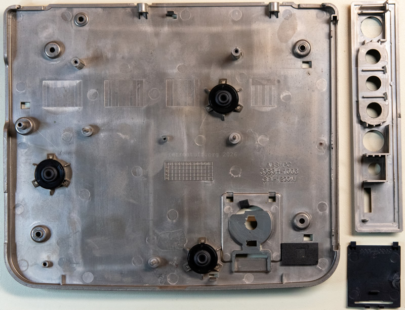
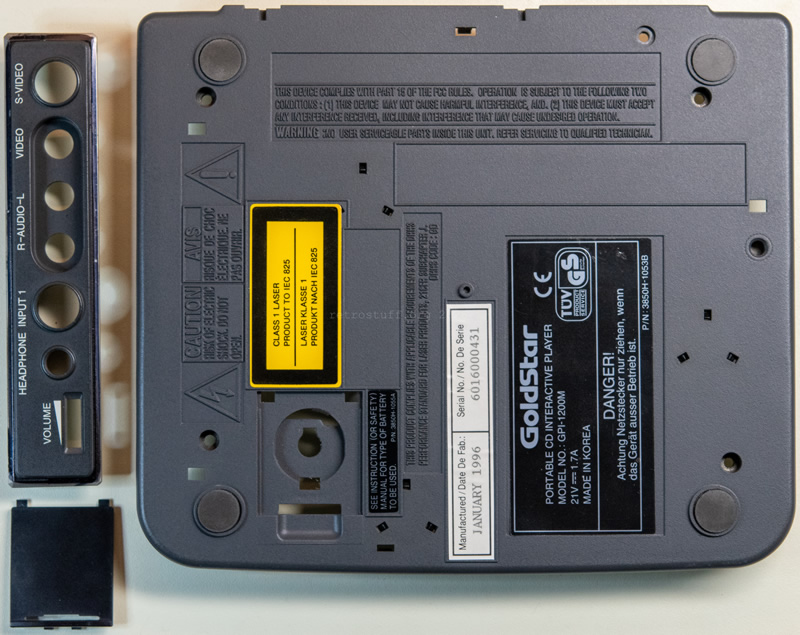
At this point, only the plastic components of the bottom case remain.
Detailed photographs of the individual PCBs are shown in the following section.
6870HE10LAA (IR PCB)
IC142 (IR receiver)
S27
0565

CN112
6 pins - to main PCB
6870HA10LAA (power PCB)
Older version. On CN503, the connection to GND was added with a solder blob (on the back, above C524).
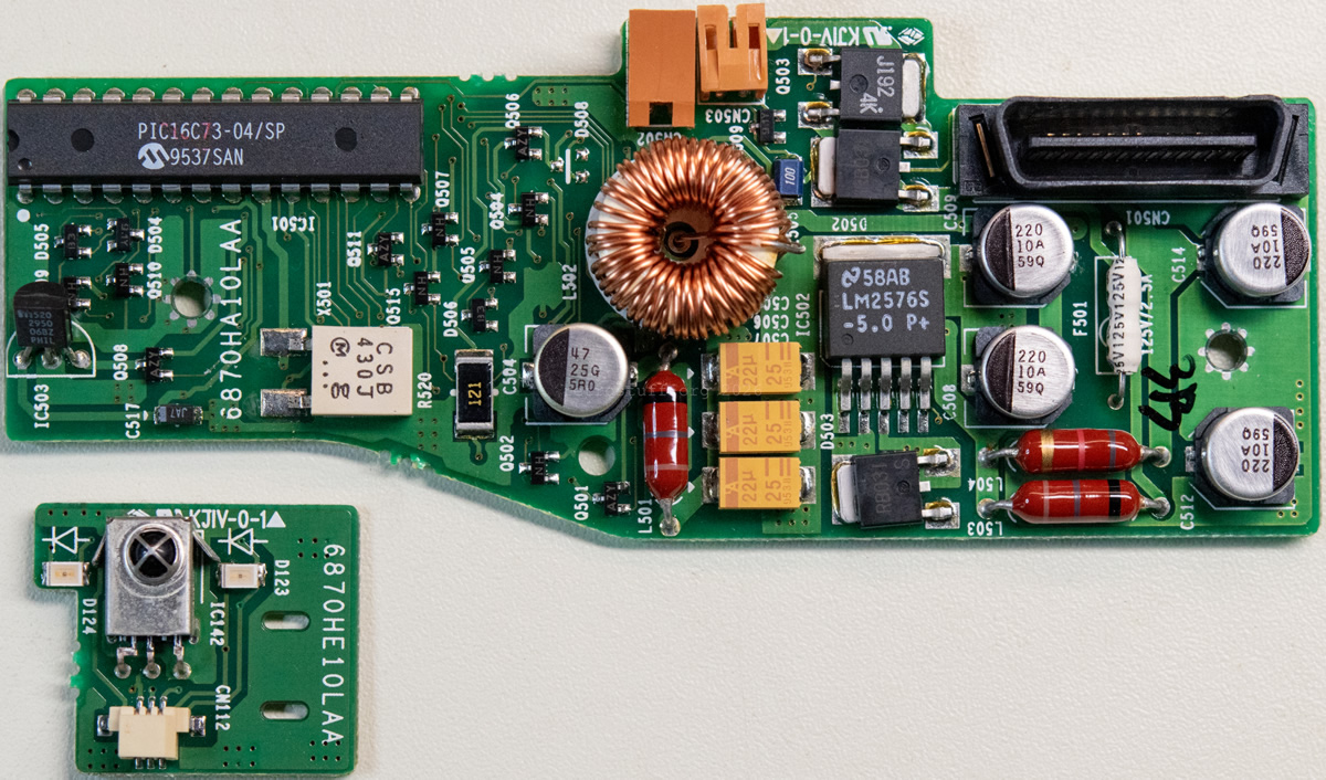
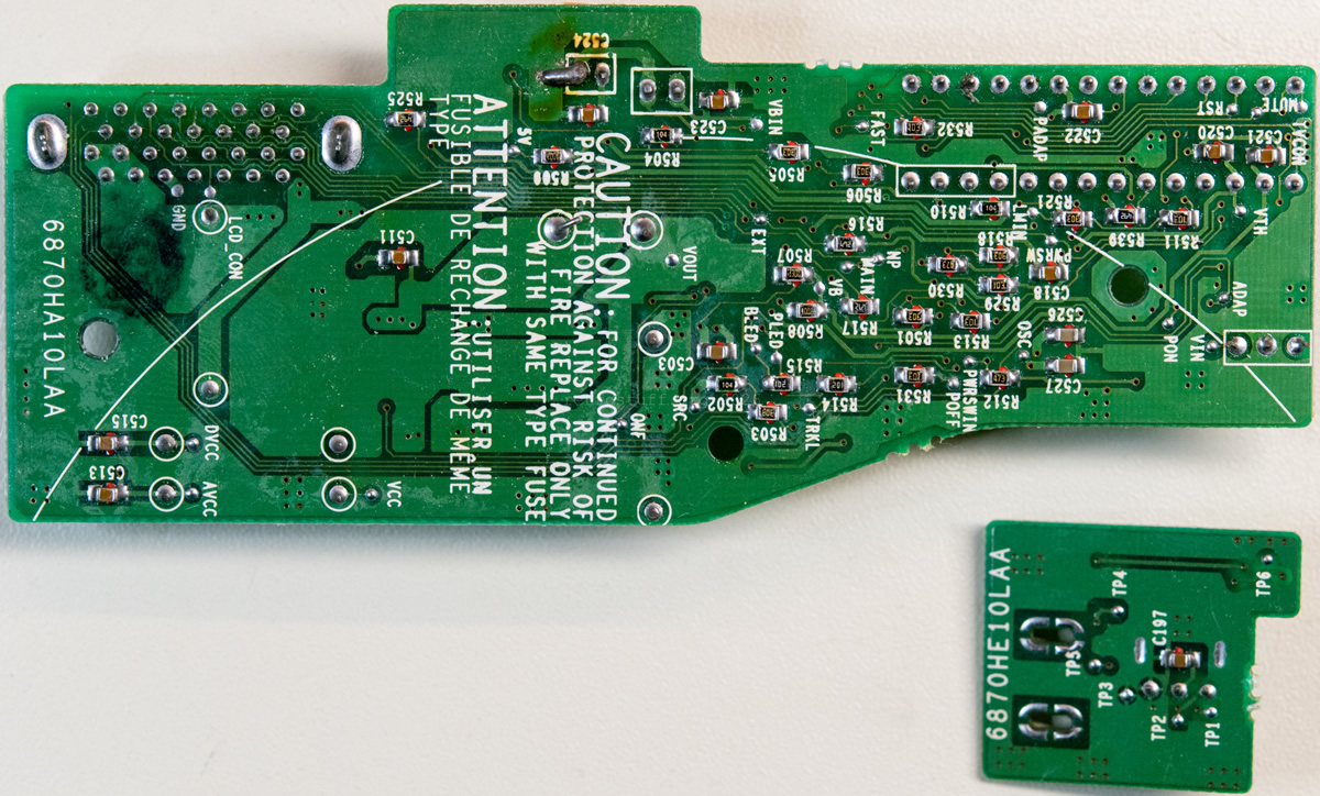
IC501
PIC16C73-04/SP
(M)9537SAN
[PIC16C73 8-Bit CMOS Microcontroller with A/D Converter]

IC502
(N) 58AB
LM2576S
-5.0  P+
[LM2576xx Series SIMPLE SWITCHER® Power Converter 3-A Step-Down Voltage Regulator]

IC503
(m) 520
2950
06BZ
PHIL
[LP2950 Voltage Regulator]

X501
CSB
430J
(M)...g

CN501
30 pins, to main PCB
[Half-pitch board-to-board connector, sim. Molex EBBI 50D, Omron XH2, Fujikura DHB]

CN502
2 pins, to 6870H-10KAA (battery +/-)

CN503
2 pins, to 6870H-10KAA (battery temp. sensor)

C504 (size E)
47
25G
5R0

C508, C509, C512, C514 (size E)
220
10A
59Q

Suspicious tantalum (size D)
C505, C506, C507
A
22mu
25
9538
6870H-10HAA (main PCB, front)
The designation 95 50 indicates that this mainboard revision is 22 calendar weeks older than that of the Philips CDI 370 mainboard.
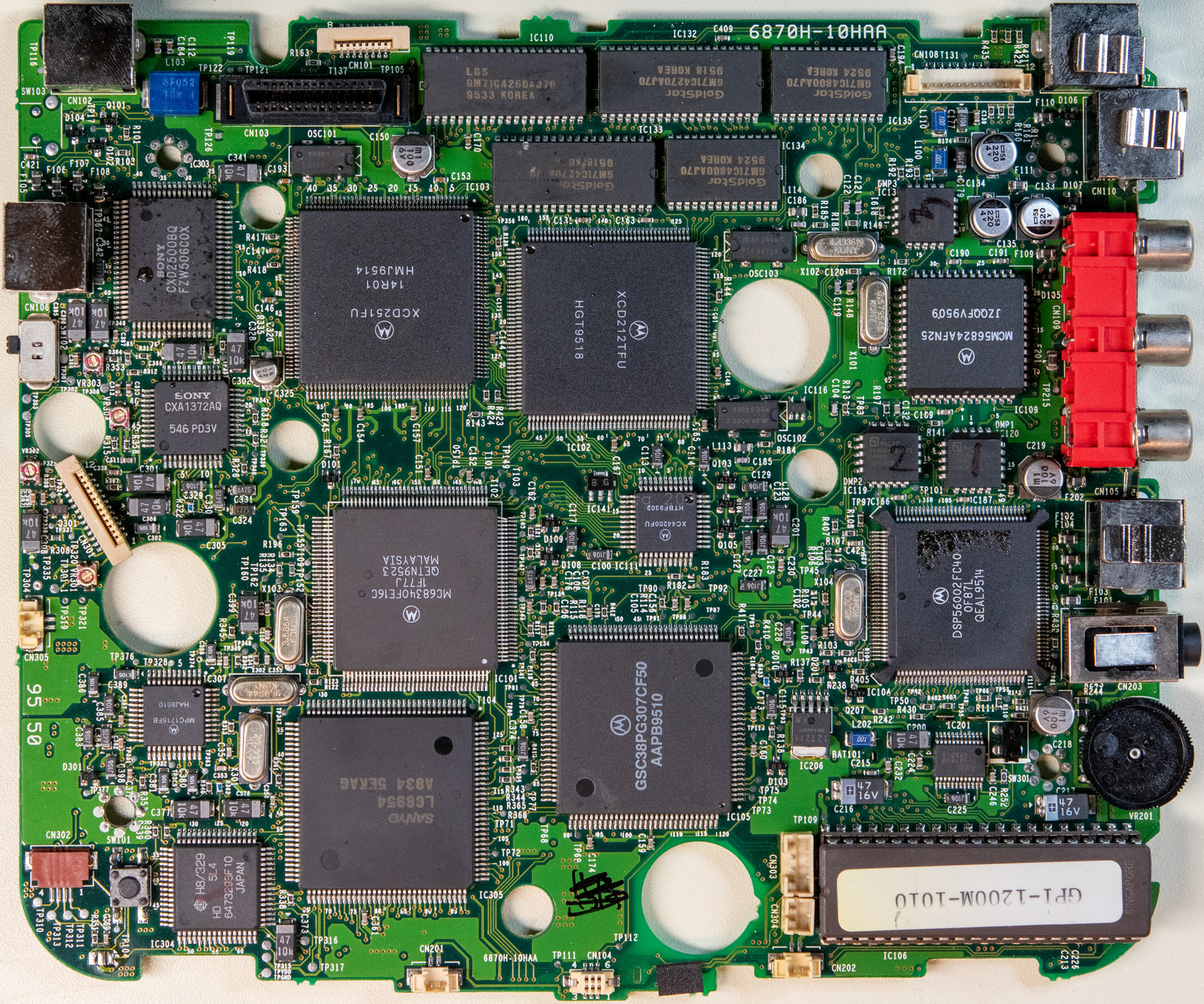
95 50

IC101
(M)
MC68340FE16C
1F77J
QETN9523
MALAYSIA
[32-BIT MICROPROCESSOR]

IC102
(M)
XCD212TFU
HGT9518
[VDSC]

IC103
(M)
XCD251FU
14R01
HMJ9514
[VMPEG]

IC104
(M)
DSP56002FC40
0F87L
QEAL9514
[DSP56002]

IC105
(M)
GSC38PG307CF50
AAPB9510

IC106
?
27C240-15
?
SINGAPORE
Sticker: GPI-1200M-1010
[256Kx16 ROM]

IC109
(M)
MCM56824AFN25
JZQQFV9509
[8Kx24 Fast SRAM]

IC110
LGS
GM71C4260AJ70
9533 KOREA
[256Kx16 DRAM]

IC111
(M)
XC44200FU
HTBF9302

IC116
E.I.

IC119 DMP2
(?) PALCE
16V8H-15JC/4
DMPP2
9548DWB L

IC120 DMP1
(?) PALCE
16V8H-15JC/4
DMPP1
9548DWB L

IC130 DMP3
(?) PALCE
16V8H-15JC/4
DMPP3
9548DWB L

IC132, IC133
GoldStar
GM71C4270AJ70
9508 KOREA
[256Kx16 DRAM]

IC134, IC135
GoldStar
GM71C4800AJ70
9524 KOREA
[512Kx8 DRAM]

IC141
8 G
[Voltage Regulator]

IC201
AKM
AK4319VM
4N521N
[STEREO D/A CONVERTER]

IC206
12TZ11
SHARP
D0 FN
[Voltage Regulator]

IC302
SONY
CXA1372AQ
546 PD3V
[RF SIGNAL PROCESSING]

IC303
SONY
CXD2500BQ
FZW506C0X
[DSP]

IC304
(Hitachi) H8/329
HD		5L4
6473298F10
JAPAN

IC305
SANYO
LC8954
A834 5EKAG
[RCHIP/ADPCM]

IC307
(M)
MPC1715FB
HAJ9510


OSC101
M 40.0000 C
PCE5460A

OSC102
M 30.0000 C
PCE5460A

OSC103
M 30.2098 C
PCE5470A

X101
3.579545
KONY

X102
4.433619
KONY

X103
3.6864
KONY

X104
40.000
KONY

X301
20.000
KONY

X302
16.9344
KONY


SW101
power

SW102
PAL/ NTSC

SW103
-not populated-

SW301
lid


CN101
FFC 8 pins, to lid buttons

CN102
Mini-DIN-5, DC INPUT

CN103
30 pins, to power PCB
[Half-pitch board-to-board connector, sim. Molex EBBI 50D, Omron XH2, Fujikura DHB]

CN104
6 pins, to IR PCB

CN105
Mini-DIN-8, INPUT 1

CN106
Mini-DIN-8, INPUT 2

CN107
Mini-DIN-6, A/V IN

CN108
12 pins, to display

CN109
3x cinch

CN110
Mini-DIN-4, S-VIDEO

CN201
2 pins, left speaker

CN202
2 pins, right speaker

CN203
3,5 mm TRS, headphone

CN301
FFC 12 pins, to CDM SF-92.5 4/12

CN302
FFC 4 pins, to CDM SF-92.5 4/12

CN303
4 pins, to CDM tracking motor + limit switch

CN304
2 pins, to CDM turntable motor

CN305
2 pins, to CDM GND


VR201
Volume

VR301, VR302, VR303, VR304
laser?


C133, C134, C135 (size C)
5a
220
4V

C150, C218, C219 (size C)
m1
100
6V

C325 (size A)
14
22
6V
leaking?
6870H-10HAA (main PCB, back)
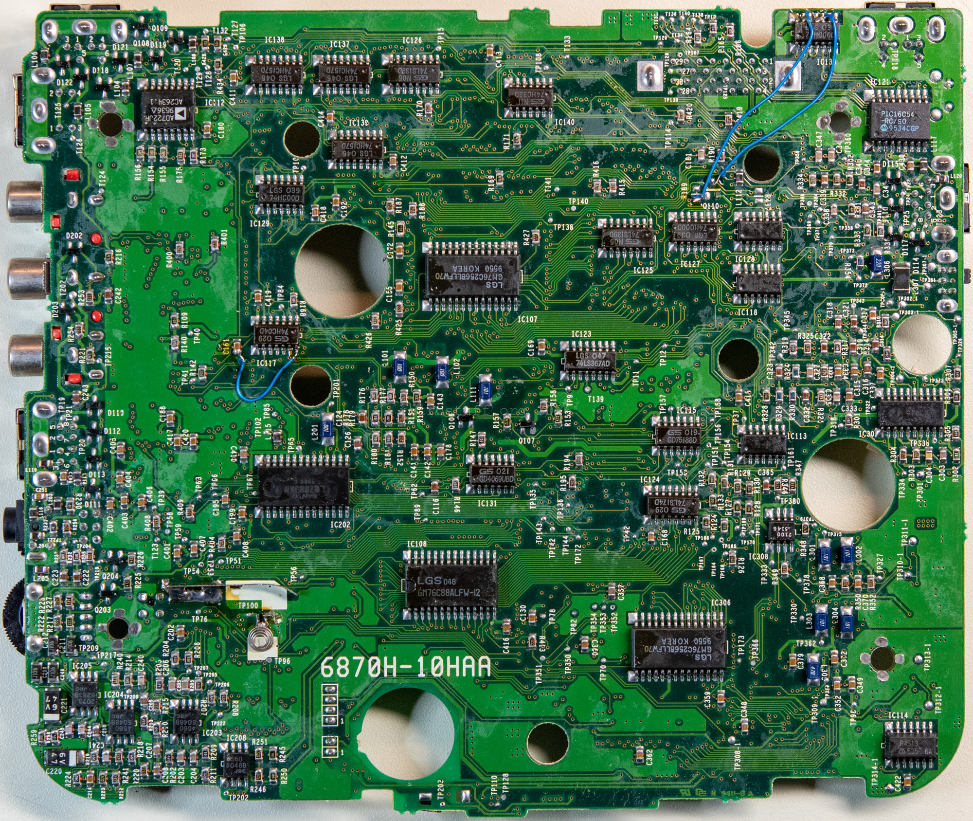
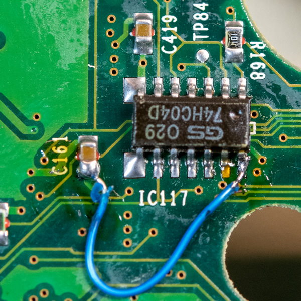
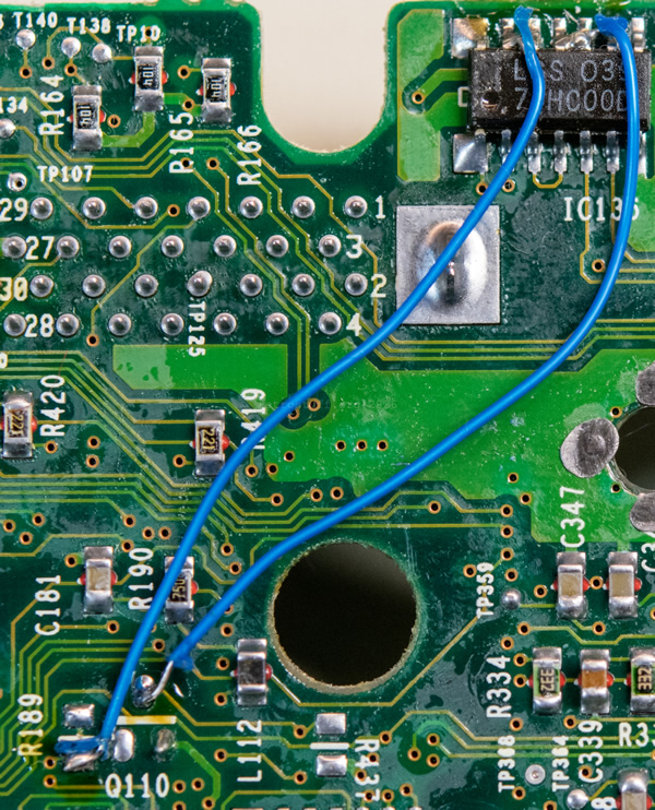
Interesting details: Bodge wires are present on IC117 and IC136.
IC107, IC306
LGS
GM76C256BLLFW70
9550 KOREA
[32Kx8 SRAM]

IC108
LGS O48
GM76C88ALFW-12
[8Kx8 SRAM]

IC112
(>) AD722JR
9536^
AC2634.1
[AD722 RGB to NTSC/PAL Encoder]

IC113
GS O21
GD75189AD
[Quadruple Line Receivers]

IC114
R4513
(M) 535 6A
[CLOCK MODULE]

IC115
GS O19
GD75188D
[Quadruple Line Drivers]

IC117
GS O29
74HC04D
[HEX INVERTER]
Bodge wire pin 14 to C161 (lower)

IC118
GS O14
74LS393D
[Dual 4-bit binary ripple counter]

IC121
PIC16C54
-RC/SO
(M) 9534 CGP

IC123
LGS O47
74LS367AD
[Hex buffer/line driver; 3-state]

IC124
GS O29
74LS174D
[Hex D-type flip-flop with reset; positive-edge trigger]

IC125, IC126
GS N05
74LS139D
[Dual 2-to-4 line decoder/demultiplexer]

IC127, IC129, IC136
LGS O39
74HC00D
[QUAD NAND GATE]
Bodge wires:
IC136 pins 10+11 to Q110 footprint (upper middle)
IC136 pins 12+13 to R139 footprint (lower)

IC128
GS O18
74LS08D
[QUAD AND GATE]

IC131
GS O21
GD4069UBD
[HEX INVERTER]

IC137, IC138, IC139 (last digit covered by via)
LGS O45
74HC157D
[Quad 2-input multiplexer]

IC140
GS N11
74HC32D
[QUAD OR GATE]

IC202
SANYO
LC7883KM
5HR0 G
[16-bit Ditial Filter and Digital-to-analog Converters for Digital Audio]

IC203, IC204, IC208
4560
5048B
JRC
[DUAL OP-AMP]

IC205
2073
5283B
JRC
[DUAL LOW VOLTAGE POWER AMPLIFIER]

IC30? (last digit covered by solder pad)
SONY
CXA1571M
510A14V
[RF Amplifier]

IC308
2100
514G
[DUAL OP-AMP]
Input ports diagnosis and repair
Both input ports fail to establish communication. The system still reacts to some incoming serial data during boot, indicating that the receive path remains operational. However, no data can be transmitted through either port.
The serial interfaces are implemented using a GD75189AD line receiver (IC113) and a GD75188D line driver (IC115). Comparison with my known-good CDI 370 mainboard showed that the GD75188 normally receives approximately +11,8 V and -8,6 V, allowing it to generate valid RS-232 output levels. On the faulty GPI-1200M board, the positive supply is completely absent, while the negative rail is unstable and measures only approximately -4.6 V.
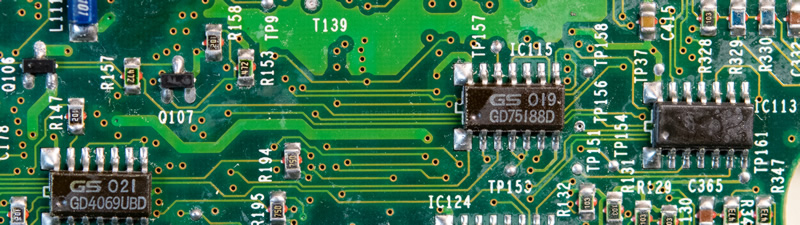
Further investigation traced the missing positive rail to the front: IC141, a SOT-89 regulator marked 8G, most likely KEC KIA78L12F linear voltage regulator. On the CDI 370 mainboard, IC141 generates approximately +11,8 V. On the GPI-1200M board, however, IC141 receives no input voltage and therefore produces no output voltage.
Tracing the supply path and comparing it with the CDI 370 showed that regulator IC141 receives its input voltage through transistors Q106 and Q107. Q106 was tested first and found to be fully functional.
Inspection of Q107 revealed something unexpected: one leg of the SOT-23 package was not soldered at all and visibly floating above the PCB. The corresponding pad was completely bare.
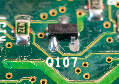
After soldering the missing Q107 connection, the +11,8 V rail immediately reappeared and both serial ports started working normally again.
A table showing the approximate voltages to expect at both input ports, as well as the line driver/receiver pins, in case you want to trace the signals:
| Mini-DIN | Signal | INPUT 1 Voltage | INPUT 1 IC pin | INPUT 2 VOLTAGE | INPUT 2 IC PIN |
|---|---|---|---|---|---|
| 1 | ./. | ./. | ./. | ./. | ./. |
| 2 | RXD | 0,067 | IC113 pin 1 (1A) | 0,067 | IC113 pin 13 (4A) |
| 3 | TXD | -7,786 | IC115 pin 6 (2Y) | -7,786 | IC115 pin 8 (3Y) |
| 4 | DTR | 0 | 0 | ||
| 5 | GND | 0 | 0 | ||
| 6 | CTS | 0,066 | IC113 pin 4 (2A) | 0,066 | IC113 pin 10 (3A) |
| 7 | RTS | 11,302 | IC115 pin 3 (1Y) | -7,779 | IC115 pin 11 (4Y) |
| 8 | +5 V | 4,956 | 4,956 |
Disassembly top case and lid
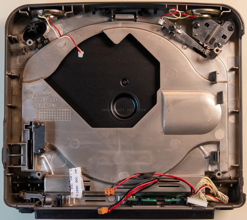
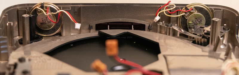
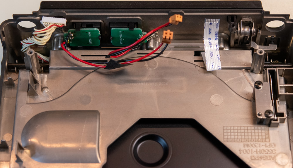
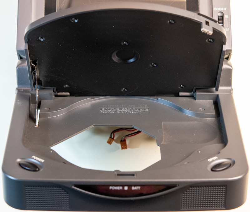
At present, there is no need to further disassemble the top case or lid, so only a few detail photos are shown here.
The speakers are labelled DAE YOUNG 32Ω. The small PCBs carrying the battery contacts are labelled 6870H-10KAA.
Disassembly, PCBs and markings (display)
To disassemble the display unit, first locate the four screws. The screw holes are covered with self-adhesive inserts made of a soft material. They can be removed easily with a fingernail and no force is required.
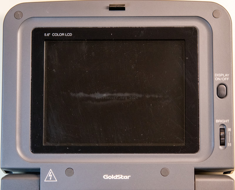
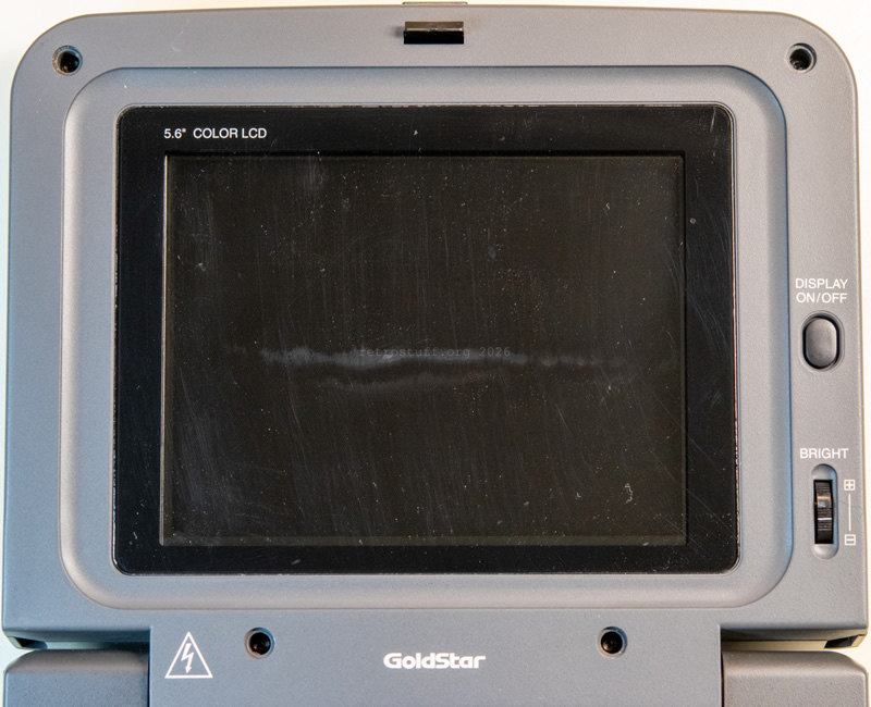
Once the screws have been removed, close the display and carefully lift off the back cover. This should come apart without force, although a plastic spudger may be helpful to separate the halves initially.
The photo below also shows the screws and the adhesive covers.
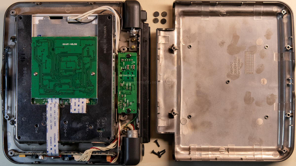
Next, remove the various PCBs one by one. Pay attention to the routing and orientation of the FFCs to make reassembly easier.
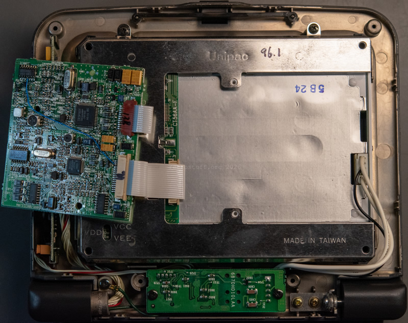
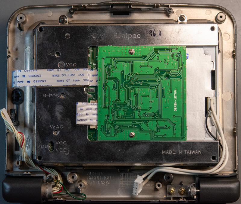
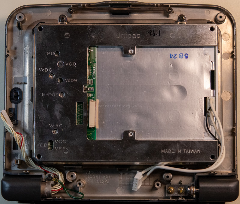
The LCD panel itself is a Unipac UP661A-1, CT56AA-F.
Since the display is working perfectly, I did not disassemble the panel further in order to avoid introducing dust into the LCD assembly. There was, however, a small amount of dust trapped behind the clear protective plastic. This was removed using a turbo air blower before reassembly.
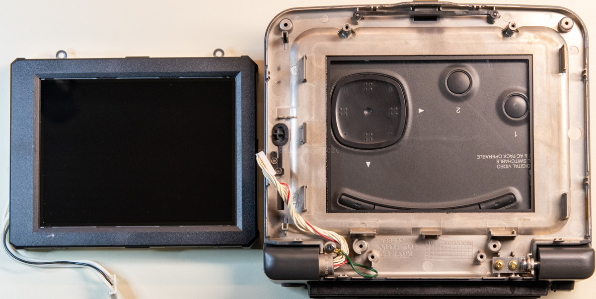
Maintenance: Hinge
While the display unit is disassembled, it is a good opportunity to check the condition of the hinge.
Over time, the original grease can dry out, making the display increasingly difficult to open and close. If left unattended, the hinge may eventually seize, putting excessive stress on the plastic mounting points and potentially breaking the areas where the hinge is screwed into the housing.
Do not remove the hinge while the display is closed. Instead, open the display to approximately 90° and then remove the screws. The display can then be pulled out from the opposite side. The cable is long enough to allow it to be moved diagonally away from the hinge.
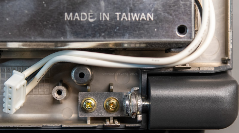
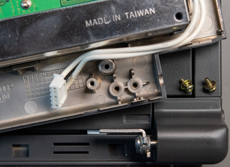
Place some paper towels or other absorbent material underneath to catch the old grease. First remove any loose dust with compressed air. Then thoroughly clean the hinge using a suitable solvent such as IPA.
Use pliers to slowly work the hinge back and forth while cleaning in order to reach as much of the mechanism as possible. The entire procedure can be carried out without removing the hinge from the body, which is convenient as the screws on that side are difficult to access.
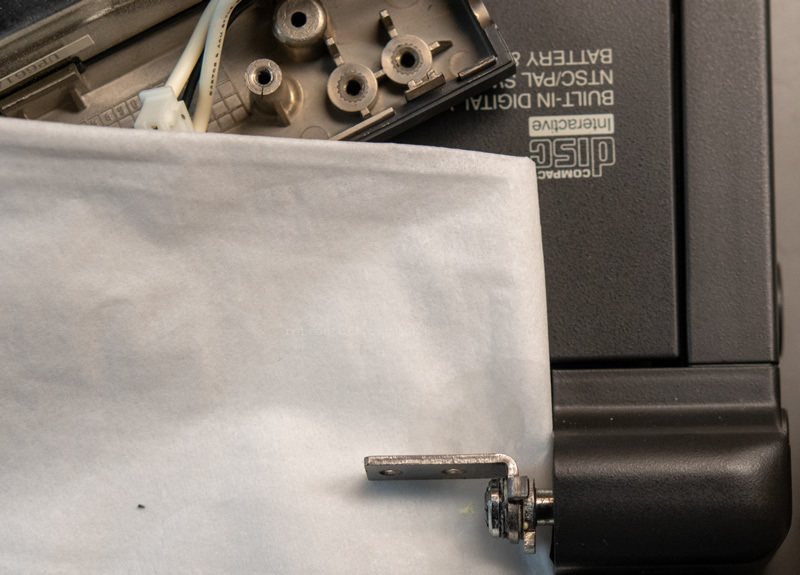
Once the old grease has been removed, re-lubricate the hinge. A viscous PTFE-based lubricant works well for this application.
Again, work the hinge back and forth with pliers while gradually applying fresh lubricant. Continue until the movement becomes reasonably smooth. At this point, the hinge can usually be operated by hand again.
Finally, return the hinge to the 90° position and reinstall it into the display assembly.
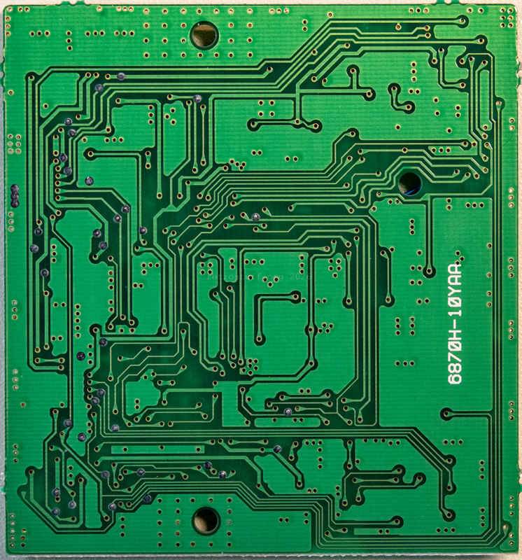
6870H-10YAA
There’s a bodge wire from IC803 to CN802.
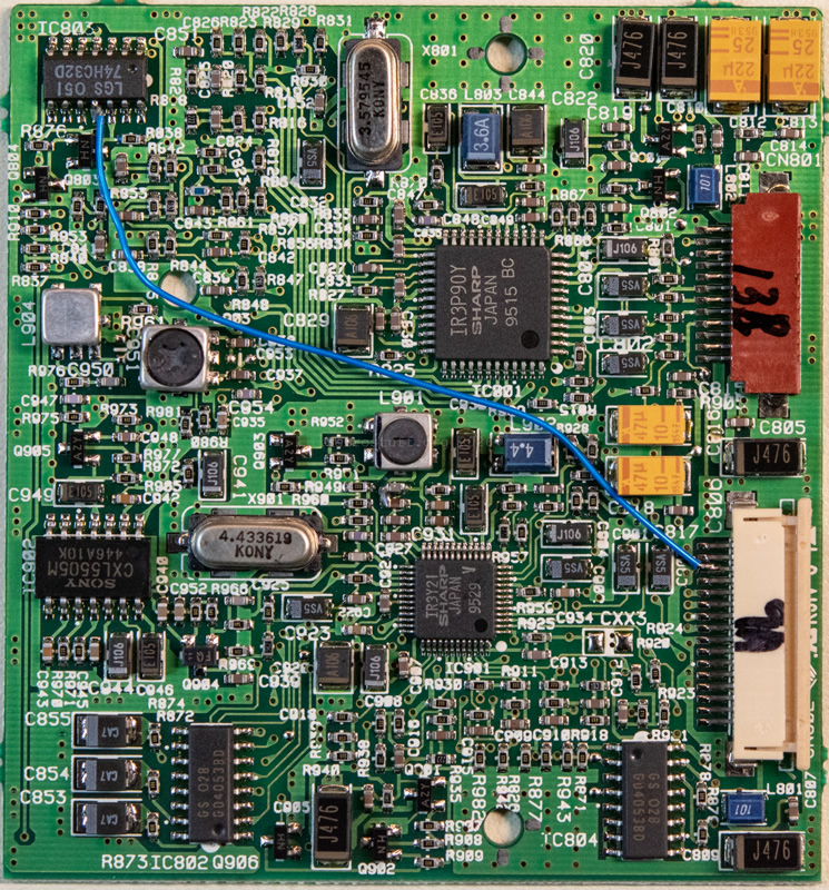
IC801
IR3P90Y
SHARP
JAPAN
9515 BC
[Video Interface IC for TFT-LCD]

IC802
GS O28
GD4053BD
[TRIPLE 2-CHANNEL ANALOG MULTIPLEXER/DEMULTIPLEXER]

IC803, IC804
LGS O51
74HC32D
[Quad 2-Input OR Gate]
Bodge wire from pin 11 to CN802 pin3

IC901
IR3Y21
SHARP
JAPAN
9529 V
[Video Interface IC for TFT-LCD]

IC902
SONY
CXL5505M
446A 10K
[CMOS-CCD 1H Delay Line for PAL]


X801
3.579545
KONY

X901
4.433619
KONY


CN801
FFC 12 pins, to 6870HC10LAA CN702

CN802
FFC 16 pins, to panel CT56AA-F JP1

C806, C816
A
47µ
10
9547
tantalum size C

C812, C813
A
22µ
25
9538
suspicious tantalum size D
6870HD10LAA
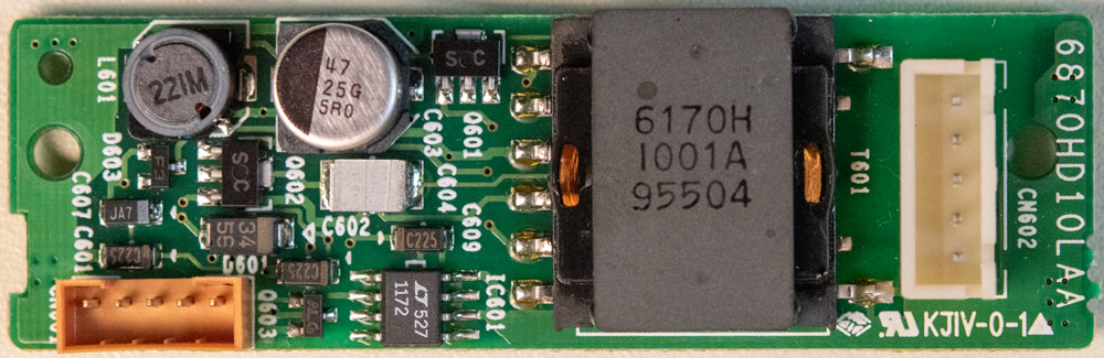
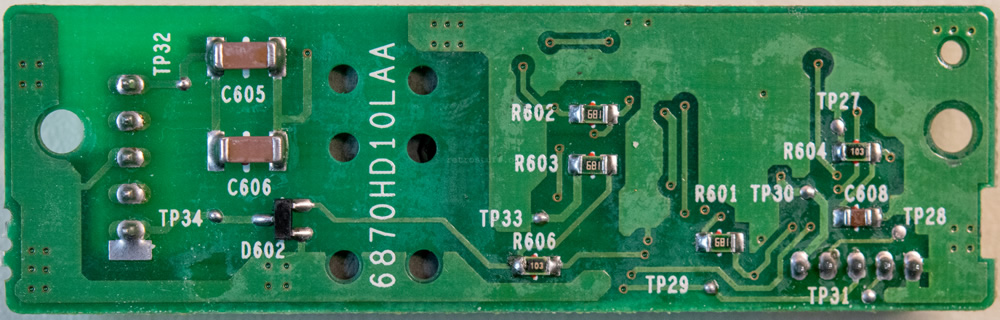
IC601
(LT) 527
1172
[LT1172 1.25A High Efficiency Switching Regulator]

Q601, Q602 (SOT-89)
S C

T601
6170H
I001A
95504

CN601
5 pins, to 6870HC10LAA CN703

CN602
5 pins, to backlight

C603 (size E)
47
25G
5R0
6870HC10LAA
Earlier revision of this PCB.


IC701
7610
525
[NJU7610 Step-Up / Flyback switching regulator IC with Over Current Protection]

IC702
GS O19
74LS74AD
[Dual D-type Positive Edge-triggered Flip-Flops (with Preset and Clear)]

IC703
LGS O37
74HC00D
[Quad 2-input NAND gate]

Q701 (SOT-89)
DC
HR
DCA75 Pro results:
NPN Silicon BJT
hFE=139 at Ic=5,01mA
Vbe=0,656V at Ib=1,00mA
Vbe=0,715V at Ib=5,00mA
VceSat=0,014V at Ic=5,0mA and Ib=1,00mA
IcLeak=0,000mA

T701
I002A
548P

CN701
12 pins, to mainboard 6870H-10HAA CN108

CN702
FFC 12 pins, to 6870H-10YAA CN801

CN703
5 pins, to 6870HD10LAA CN601

SW701
display on/off

VR701
brightness


C702, C704, C709, C711
A
22µ
25
9538
suspicious tantalum size D

C713, C715 (size C)
m1
100
6V

C717
A
47µ
10
9547
tantalum size C

C719 (size E)
100
10G
59R
GIA-110 (power supply unit)
The power supply unit is surprisingly difficult to disassemble. The first challenge is locating the only screw securing the enclosure. It is hidden directly beneath the product label.
MODEL NO.:GIA-110
INPUT:100-240V~,50/60Hz, 45W  OUTPUT:21V⎓1.7A
P/N: 3850H-1058C
I was able to lift the label using IPA and careful prying. Underneath, I also found the handwritten marking 480296A.
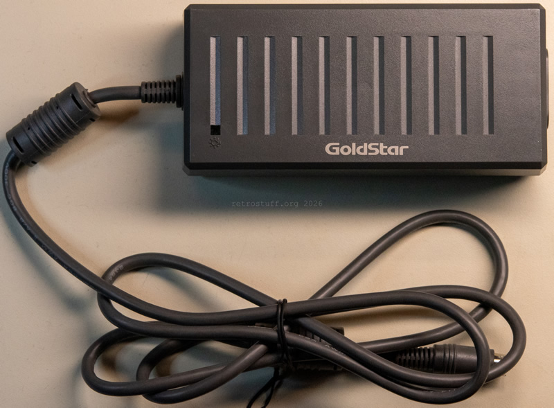
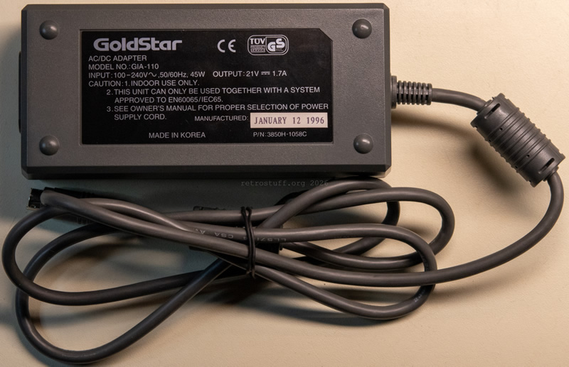
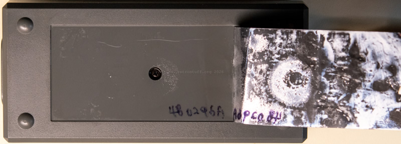
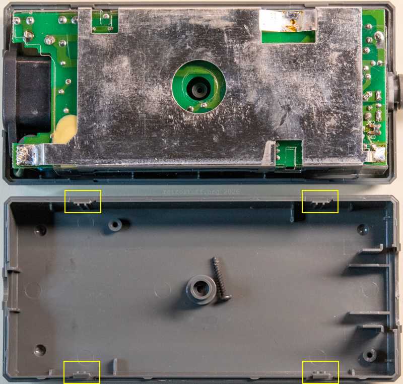
After removing the screw, the two halves of the enclosure can be separated. Four plastic hooks need to be released first; this can be done easily using a spudger. The PSU assembly can then be removed from the plastic housing.
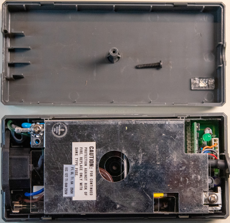
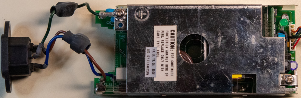
The next obstacle is the sheet-metal shielding. Before it can be removed, the three marked ground connections must be desoldered. A higher soldering temperature and a larger tip may be required.
Be particularly careful around the upper-left solder joint, as it is located directly next to IC2.
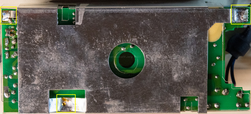
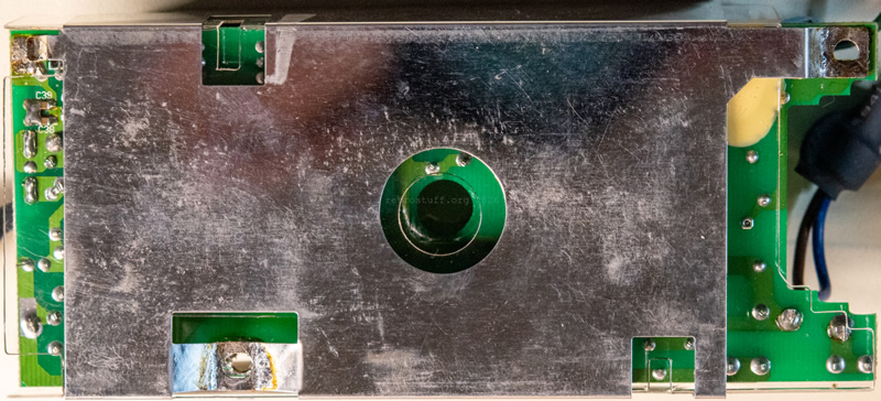
Once the lower side has been freed, turn the assembly over and remove the screw in the lower-right corner. This separates the shield from the heatsink and allows it to be opened.
Removing the upper-left screw securing the ground wire is optional, but it makes handling the shield considerably easier. Note that the nut on the opposite side must be held while loosening the screw.
The sheet-metal shield can then be bent open sufficiently to slide it off.
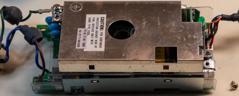
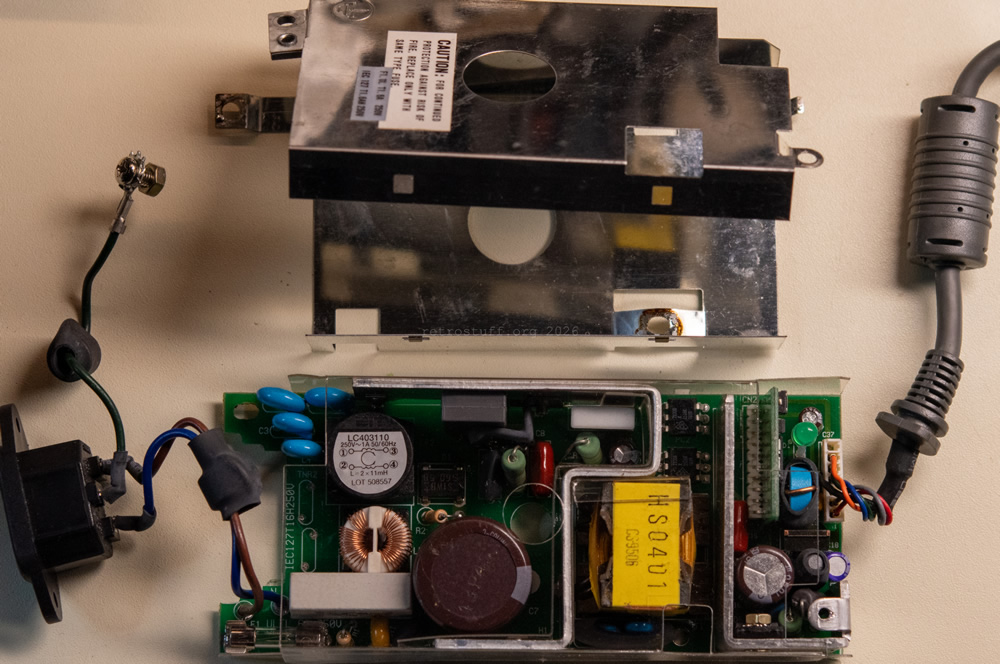
If you thought this would finally provide access to the PCB, think again.
A plastic enclosure remains, which is glued to the underside of the board. I managed to separate it by carefully sliding a scalpel between the PCB and the plastic and cutting through the adhesive.
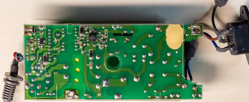
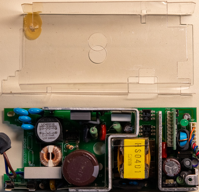
Finally, full access to the PCB and components:
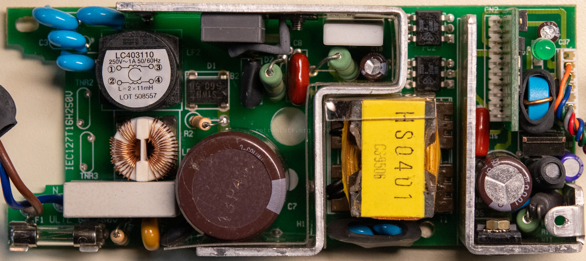
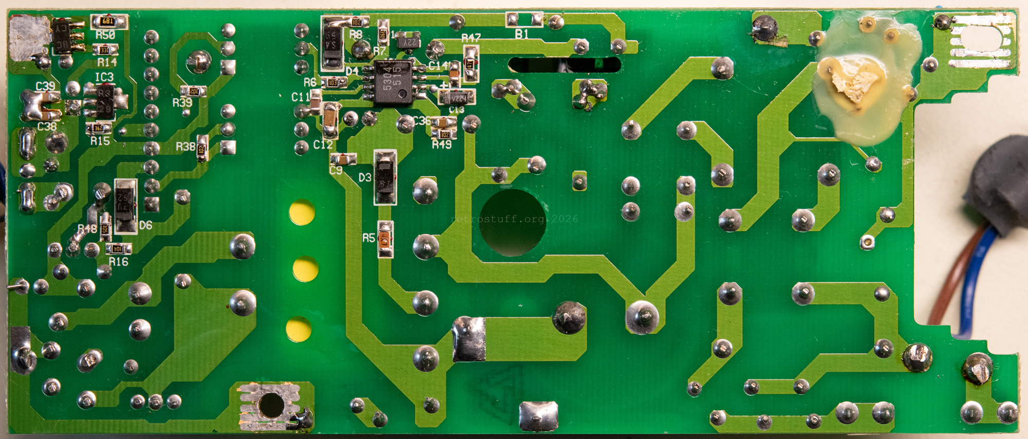
Interesting details: photos of the daughterboard soldered to CN2, and of IC1, where pin 1 has clearly been bent back and soldered to pin 2.
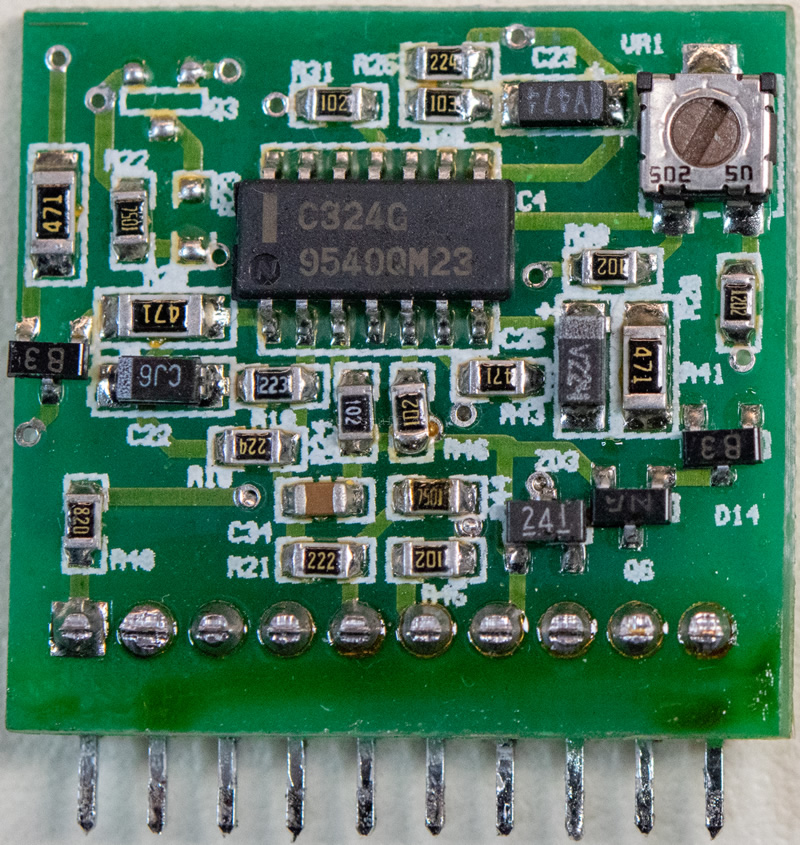
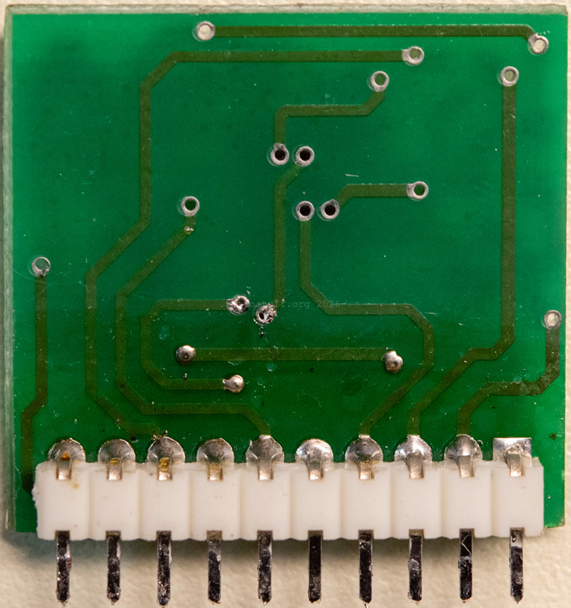
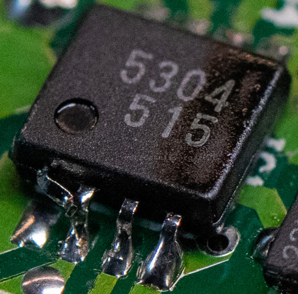
Markings
Markings of the ICs and other important components.
If you have made it this far, it is worth carefully inspecting the electrolytic capacitors. C10 was visibly leaking, while C18 and C37 also appeared suspicious. Despite this, all capacitors still measured within specification.
IC1
5304
515
[FP5304AP Bipolar IC For Switching Power Supply Control]

IC2
8C
CY

IC3
93
29

IC4 (on sub PCB)
C324G
9540QM23
[µPC324 LOW POWER QUAD OPERATIONAL AMPLIFIER]

PC1, PC2
IS206
X
I515K
0884
(DVE)
[OPTICALLY COUPLED ISOLATOR]


VR1 (on sub PCB)
502 50

CN1
7 pins, to Mini-DIN-5
1 +21 V - red - 2
2 +21 V - grey - 1
3 GND - n.c.
4 GND - blue - 4
5 GND - green - 3
6 +5 V - orange - 5
7 +5 V - n.c.

CN2
10 pins, daughterboard


F1
250V1,6A
51NM(J)(UL)(SA)


C7
(SAMYOUNG)KMH
CE-W
100µF  400WV
NEGATIVE BLACK
(M)105°C
13P4S

C10
(.)KME
50V
33µF
47
N(4)
(M)105°C
leaking

C16
(SAMYOUNG)SXE
25V
1000µF
9541
(M)105°C

C18
SANYO
10
25
OS-CON
73 105°C

C37
(.)KME
16V 10µF
(M)105°C
50
D4
To-Do
- Disassemble and analyse the battery pack
- Inspect and replace suspicious capacitors (SMD electrolytic and tantalum types)
History
2026-10-18: Initial WIP Page published
2026-10-24: Component markings updated and input ports repaired. Service Shell information added
2026-10-25: Display unit disassembled and component markings updated
2026-10-27: Input port data added
2026-11-01: Power supply unit disassembled and component markings added