
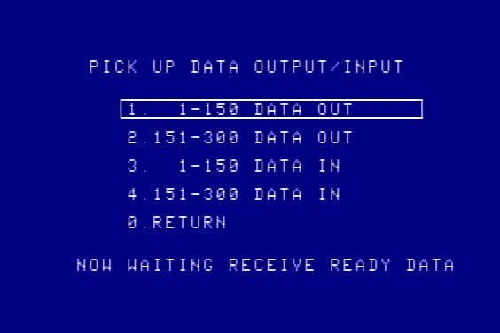
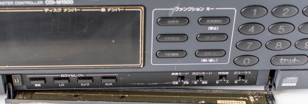
Master controller for Nikkodo / BMB CD-i karaoke systems. It is similar to the Philips CDI 181 MultiMedia Controller (JNMS). The mainboards of these units were made by Kyocera. They all lack optical disc drives and require additional units (e.g. CDI 180 for JNMS and CDI-A1500 for BMB).
So far, four different hardware generations have been found, and there may be more. The hardware has evolved from being very similar to JNMS to something that hasn’t been seen in other CD-i players. To identify different CDI-M1500 mainboards/generations, I use the first character of the serial number:
- CDI-M1500 A unit – mainboard PDCDG4001D
- CDI-M1500 L unit – mainboard PDCDG4002B
- V unit – mainboard PDCDG4003B (this WIP Page)
- VI-M450 unit – mainboard PDCDG4004A
- Resources
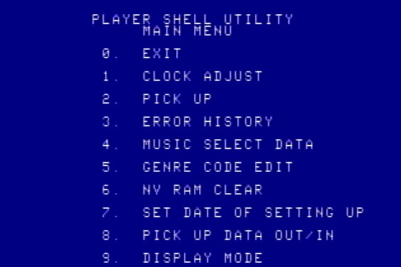
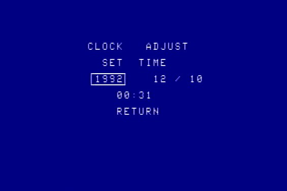
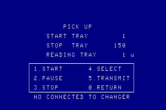
- Player shell
- System ROM
- PCBs and markings
- PSU Nichicon CI-1PS
- Repairs done
- Credits
- History
Resources
- Service manual: N/A
- Previous listings with more hardware
- BMB company history
Player shell

System ROM
For a while, it wasn’t clear whether I would ever be able to boot this unit — the system ROM sockets U26 and U27 were empty. However, it turned out that U110 (marked 62434FAD76) was a Hitachi HN62434FA 524288-word x 8-bit mask ROM. I was then able to dump it using an MX27C4100 chip driver.
This mainboard accepts two types of system ROM. When SW3 is closed, it connects U110 pin 10 (CE).
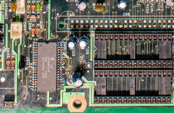
If SW3 is open, two 256 x 8-bit CMOS EPROMs can be used in U26 and U27. However, the system ROMs of the A-unit are not compatible with the V-unit due to the different hardware. I accidentally lifted two solder pads when removing U110, so I had to rewire them.
Modules and checksums:
  Addr     Size      Owner    Perm Type Revs  Ed #  Crc   Module name
-------- -------- ----------- ---- ---- ---- ----- ------ ------------
00001054    26650     0.0     0555 Sys  a000    83 090798 kernel
0000786e      350     0.0     0555 Sys  8002    22 b5e45c init
000079cc     1106     0.0     0555 Sys  a013    19 f6e0d1 rp5c15
00007e1e      160     0.0     0777 5    8001     1 eb9bbd csd
00007ebe     4808     0.0     0555 Sys  a000    29 70e9a8 csdinit
00009186    18082    10.48    0555 Trap c00a     6 5f673d cio
0000d828     7798     1.0     0555 Trap c001    13 46c5dc math
0000f69e     2270     0.0     0555 Fman a000    35 d6a976 pipeman
0000ff7c     5592     0.0     0555 Fman a000    17 63023d nrf
00011554     4510     0.0     0555 Fman a003    96 a4d145 cdfm
000126f2     2852     0.0     0555 Fman a010    36 f247db ucm
00013216      172     0.0     0555 Driv a000     1 407f81 null
000132c2      774     0.0     0555 Driv a001     6 81a3e9 nvdrv
000135c8    11994     0.0     0555 Driv a001    84 c4c873 cddrvk
000164a2    66640     0.0     0555 Driv a011    50 c887d3 video
000268f2     2610     0.0     0555 Driv a00c    12 6b4b6f ptrdrv
00027324      218     0.0     0555 Driv a000     1 5aa9f3 nill
000273fe     2018     0.0     0555 Driv a01a    26 ce407e env68681
00027be0     1730     0.0     0555 Driv a012    18 84e637 tc68681
000282a2     2720     0.0     0555 Driv a001     1 d58796 comdrv
00028d42      102     0.0     0555 Desc 8000     2 cf450e pipe
00028da8       94     0.0     0555 Desc 8000     1 f54010 nvr
00028e06      130     0.0     0555 Desc 8000     1 8bb43e cd
00028e88      130     0.0     0555 Desc 8000     1 71e401 ap
00028f0a      130     0.0     0555 Desc 8002     1 db1f8f vid
00028f8c      128     0.0     0555 Desc 8000     1 4cdea4 ptr
0002900c      118     0.0     0555 Desc 8020     2 be7d14 nil
00029082      132     0.0     0555 Desc 8000     1 55df3a env
00029106      130     0.0     0555 Desc 8000     1 30a5e2 tc
00029188      128     0.0     0555 Desc 8000     1 44901b cmd
00029208     2992     0.0     0555 Data 8020     1 191a59 FONT8X8
00029db8     3424     0.0     0555 Data 8001     1 7941a6 stop.cl7
0002ab18    95048     0.0     0555 Prog c001     7 67fb3e psci17
00041e60     1798     0.0     0555 Prog c002     7 41174a mount
00042566    24208     0.0     0555 Prog c001     9 bae4c6 cdg_aplk
000483f6    48418   300.302   0555 Prog 8006    22 13bb00 KARAOKE$.NK1
00054118    27362     0.0     0555 Prog 8001     7 154f9e ps_aging
0005abfa    92276     0.0     0555 Data 8001     1 faeb0a stx.dyuv

    File             Addr    Size    Type             Description
------------------ -------- ------ ------------------ ------------
cdim1500v00.rom    00000000   512K cdim1500v.rom      BMB CDI-M1500 V system ROM
cdim1500v00.rom    00000000   512K cdim1500v.mdl      BMB CDI-M1500 V Auto Master Controller
cdim1500v00.rom    00000000   512K cdim1500v.brd      BMB CDI-M1500 V board
cdim1500v00.rom    00000000   512K cdim1500v.sum      Sum: BE79:1A30
cdim1500v00.rom    00000000   512K cdim1500v.crc      CRC: 24D21D7F
cdim1500v00.rom    00000000   512K cdim1500v.md5      MD5: 44B32B3D97C503212ABE40A77DBDB3D0
An image (stx.dyuv) found in the system ROM, possibly for calibration purposes.
PCBs and markings
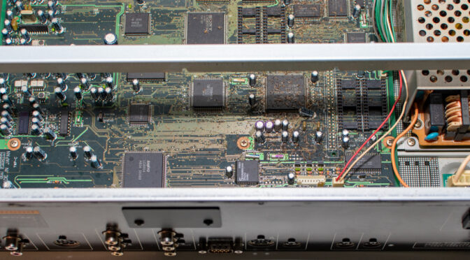
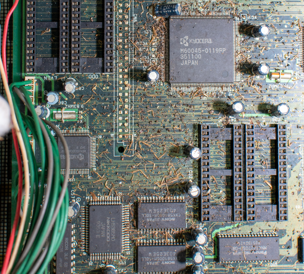
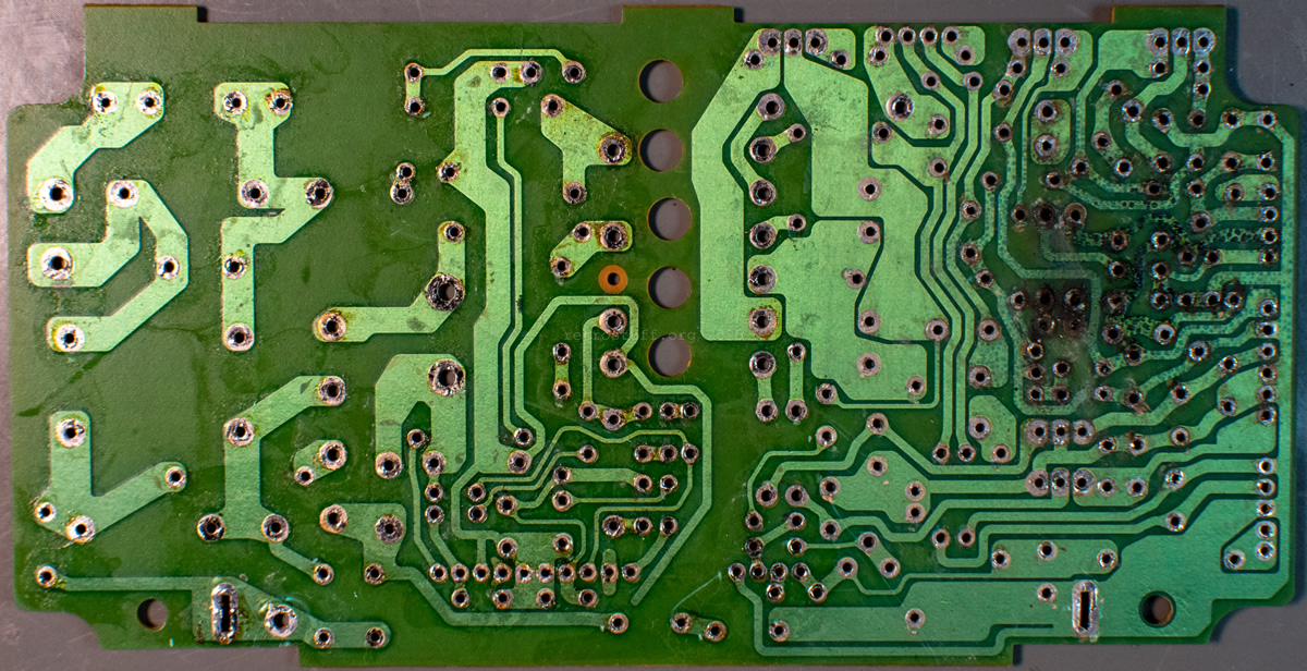
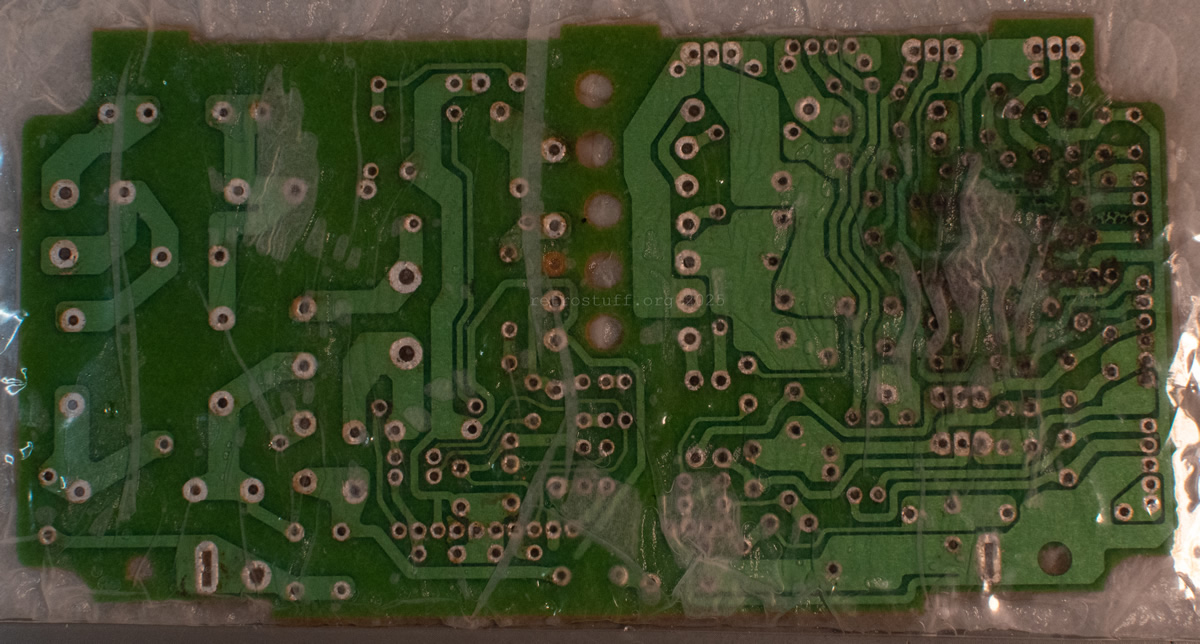
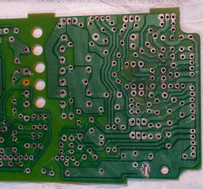
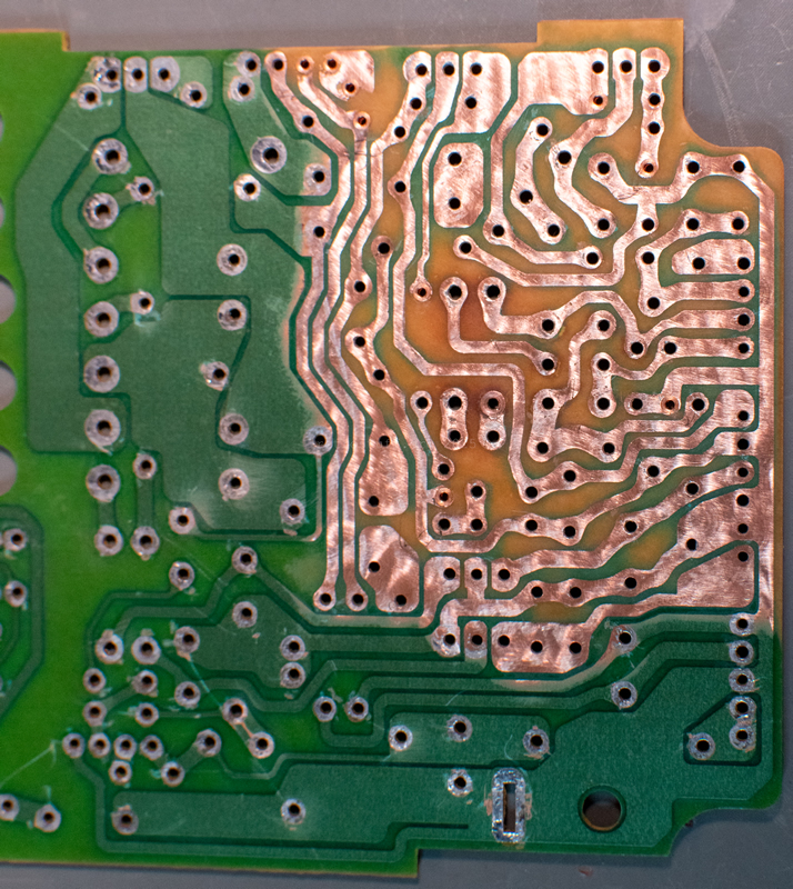
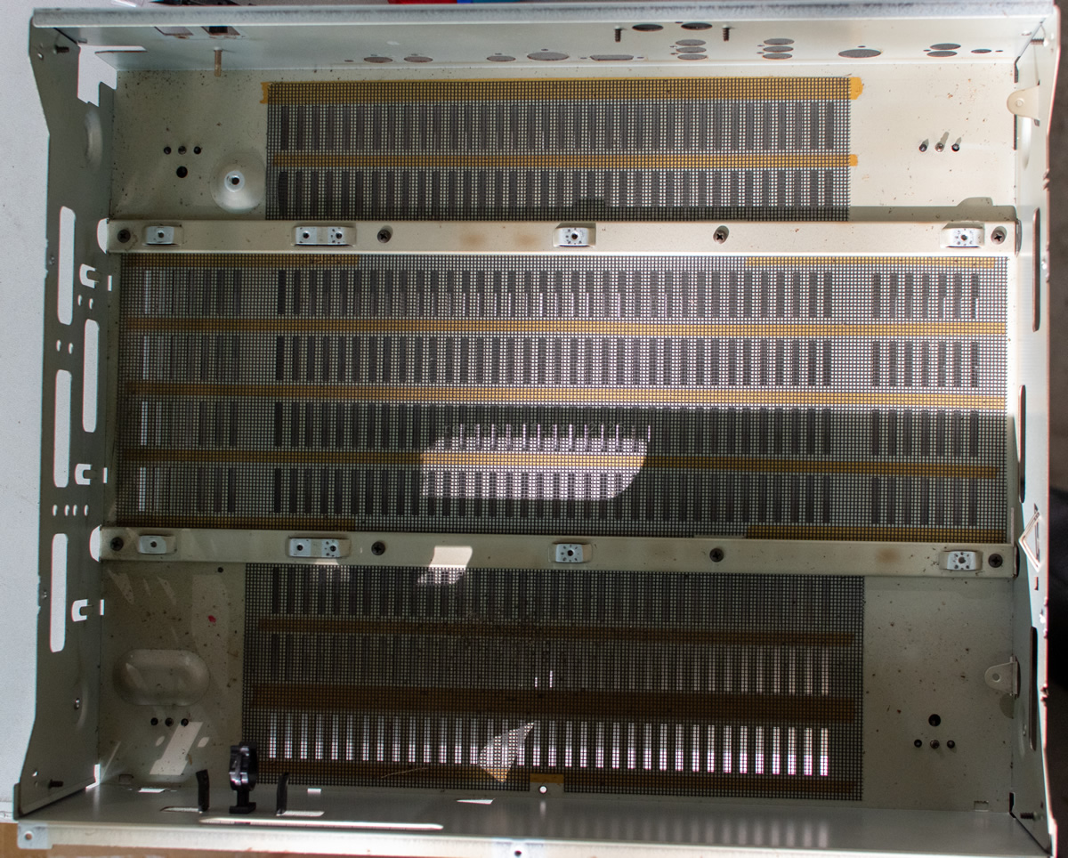
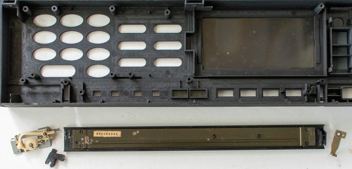
This unit is also known as the insect unit – the following pictures show what I found inside (I cleaned it thoroughly afterwards).
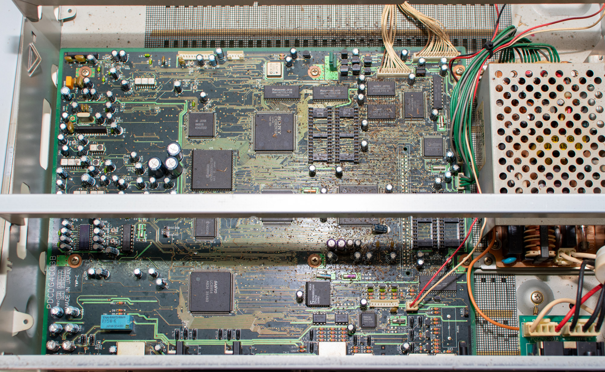
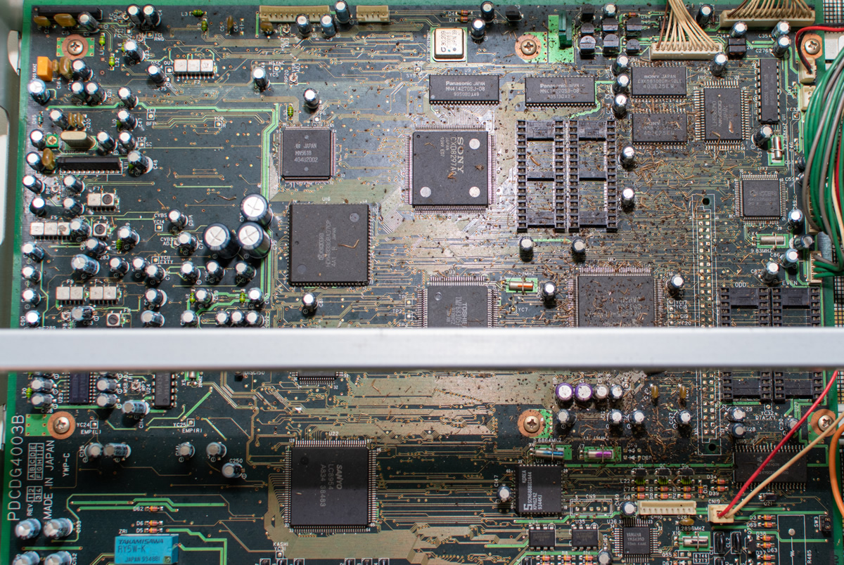
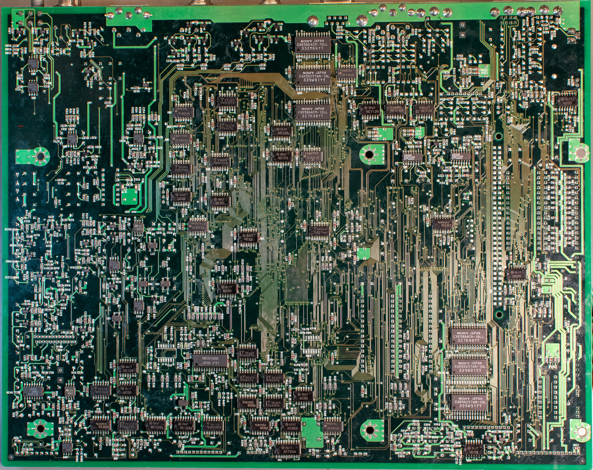
PDCDG4003B (mainboard, front)
It looks so much better after cleaning:
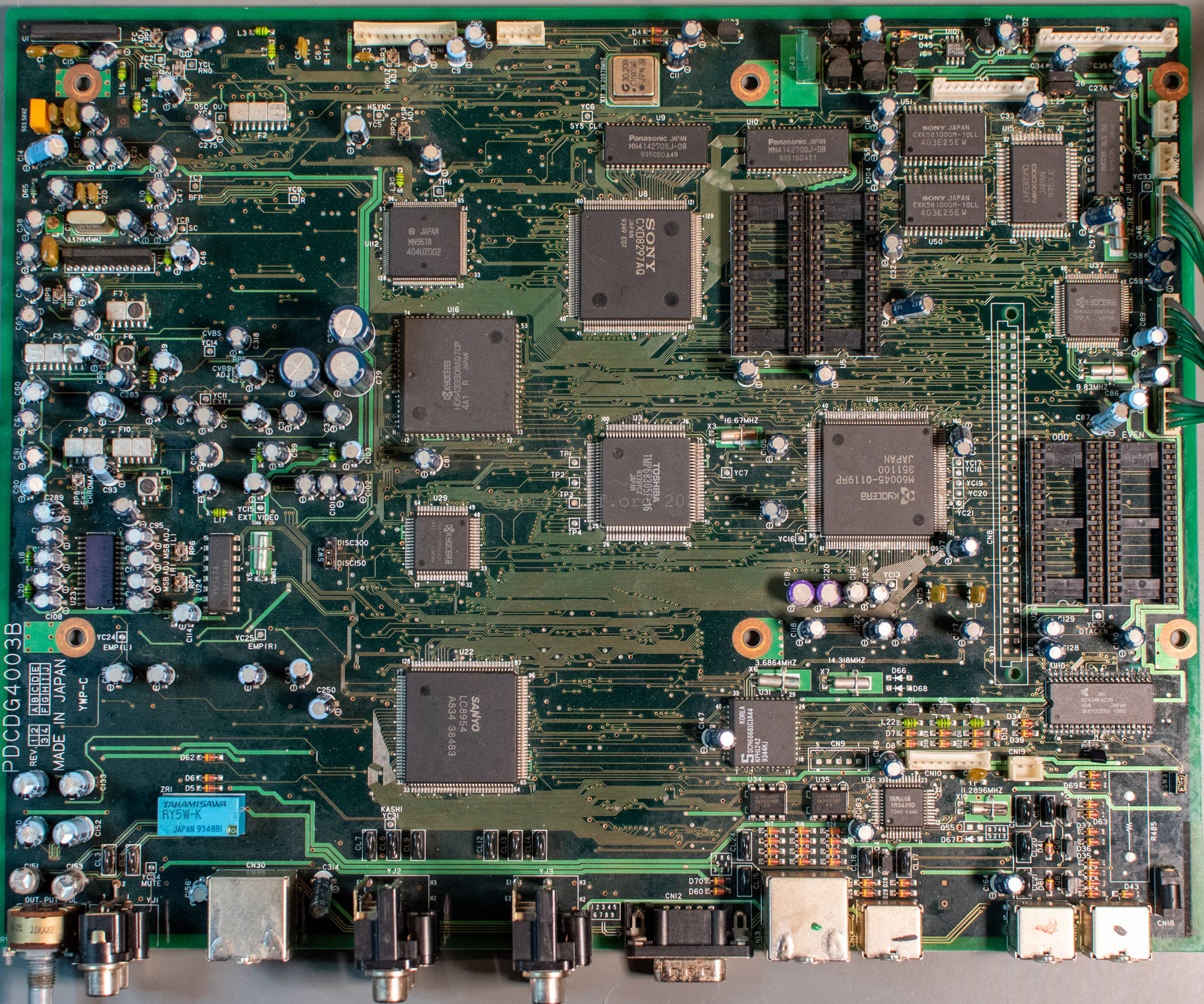
U1
TOSHIBA 9346H
TC5081AP JAPAN
[PHASE COMPARATOR]
U2
(ミツミ)350
T520C
[For System Resetting | Monolithic IC PST520 Series]
U3
TOSHIBA
TMP68305F-16
9339YCZ
JAPAN
[32-BIT MICROPROCESSOR]
U4 (empty)
U5 (empty)
U8
SONY
CXD8297AQ
JAPAN
9349 E07
[DUAL VSC]
U9
Panasonic JAPAN
MN414270SJ-08
9350BDA49
[256Kx16 DRAM]
U10
Panasonic JAPAN
MN414270SJ-08
9351BDA21
[256Kx16 DRAM]
U11
RICOH 35 68
RP5C15 JAPAN
[RTC]
U12
BA7230LS
352 126
[NTSC color TV signal encoder]
U15
LH5385M0
NIKKODO
JAPAN
9353 E
[???]
U16
KYOCERA
HD6433308A97CP
4A1 R JAPAN
[16-BIT MICROPROCESSOR]
U19
KYOCERA
M60045-0119FP
351100
JAPAN
U22
SANYO
LC8954
A834 38384
[RCHIP/ADPCM]
U23
(BB)(R)
PCM1700U
9343
CX2058
[Dual 18-Bit Monolithic Audio DIGITAL-TO-ANALOG CONVERTER]
U24
YM3434
9346 HABB
[2-Channel 8-times Oversampling Digital Filter]
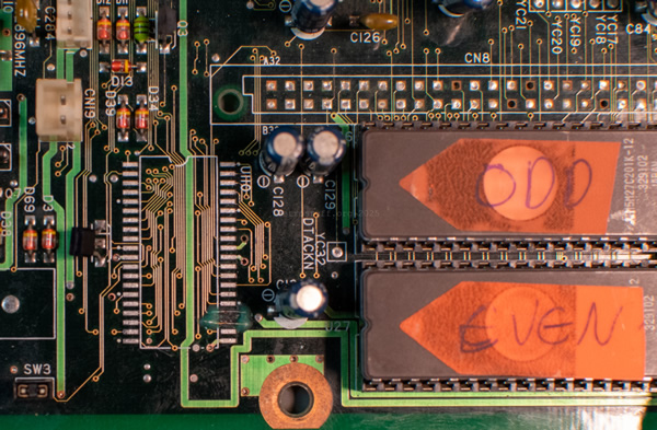
U26 ODD (empty)
U27 EVEN (empty)
U29
KYOCERA
HD6433258A83F
4A2 JAPAN
[? Hitachi Single-Chip Microcomputer HD6433258F64 ?]
U31
KOREA
(S) SCN68681C1A44
KPH1242
9344KJ
[DUART]
U34
(Ti) 3503ZBT
SN75179BP
BB
[DIFFERENTIAL DRIVER/RECEIVER]
U35
(Ti) 3503ZBT
SN75179BP
BB
[DIFFERENTIAL DRIVER/RECEIVER]
U36
YAMAHA
YM3436D
9346 KAAK
[DIF RECEIVER]
U37
KYOCERA
HD6433308R76F
3M2 R JAPAN
[? Hitachi Single-Chip Microcomputer HD6433308 ?]
U50
SONY JAPAN
CXK581000M-10LL
402E25EW
[128Kx8 SRAM]
U51
SONY JAPAN
CXK581000M-10LL
403E25EW
[128Kx8 SRAM]
U100
M5237L
2704
[3-TERMINAL ADJUSTABLE REGULATOR]
U101
NE555
(S)19W11
201KM
[PRECISION TIMER]
U103
(ミツミ)350
T520C
[For System Resetting | Monolithic IC PST520 Series]
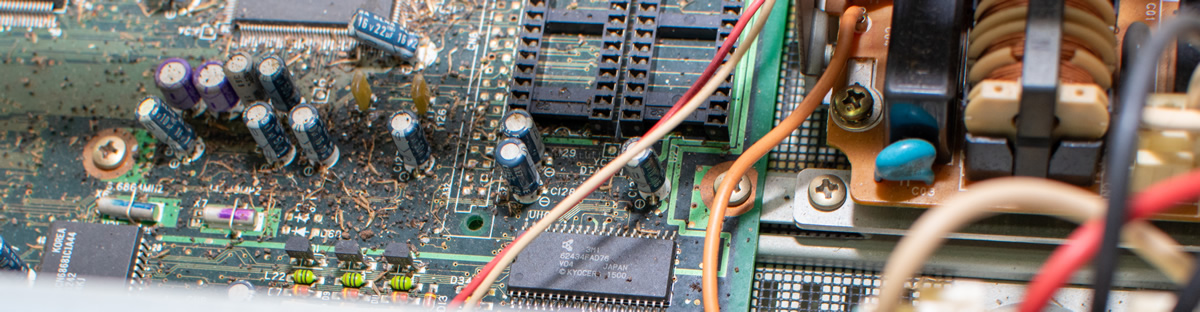
U110
3M1
62434FAD76
V04 JAPAN
(C) KYOCERA 1500
[HN624334FA 262,144-word x 16-bit / 524,288-word x 8-bit CMOS Programmable Mask ROM]
U112
(M) JAPAN
MN5618
404U2D02
[VSR???]Crystals
CX1 503,5 kHz
CSB
503F2
CH? M

X1 3,579545 MHz
X2 32,768 kHz
X3 16,67 MHz
X4 9,83 MHz
X5 20 MHz
X6 3,6864 MHz
X7 14,318 MHz
X10 11,2896 MHz

X11 30,20979 MHz
(G?) 30.209
C100ES
(dot) JPN 39
Test points
TP1 - near U3
TP2 - near U3
TP3 - near U3
TP4 - near U3
TP6 - near U112

YC1 RNG - near RP2
YC2 FC - near RP1
YC3 BFP
YC4 OSC OUT
YC5 HSYNC - near RP20
YC6 SYS CLK - near X11
YC7 - near U3, X3
YC9 R
YC11 EXTY - near RP5
YC13 - near U19
YC14 CVBS - near RP5
YC15 EXT VIDEO - near X5
YC16 - near U19
YC17 - near U19
YC18 - near U19
YC19 - near U19
YC20 - near U19
YC21 - near U19
YC24 EMP(L) - near U23
YC25 EMP(R) - near U24
YC31 KASHI - near YJ2
YC32 DTACKN - near U26/U27
YC33 - near CN5, CN20, U11, X2
YC34 MUTE - near YJ1
Connectors, pots, jumpers, switches…
CN1 12 pin
CN2 16 pin -> to VFD board CN602
CN3 14 pin -> to VFD board CN601
CN4 3 pin -> to battery CR17335SE
CN5 5 pin -> to PSU CN2
CN6 6 pin -> to PSU CN3
CN7 4 pin -> to PSU CN4
CN8 2x 32 pin (unpopulated)
CN9 5 pin (unpopulated)
CN10 9 pin
CN19 2 pin -> to power switch
CN20 3 pin
CN21 5 pin
RP1 FC ADJ
RP2 RNG ADJ
RP3 HOLIZ ADJ
RP5 CVBS ADJ
RP6 MSB ADJ (L)
RP7 MSB ADJ (R)
RP8 EXT CHROMA
RP9 BURST
RP20 VSR ADJ
SW2 DISC150 / DISC300 (150 selected)
SW3 (jumper closed) -> U110 pin 10 (CE)
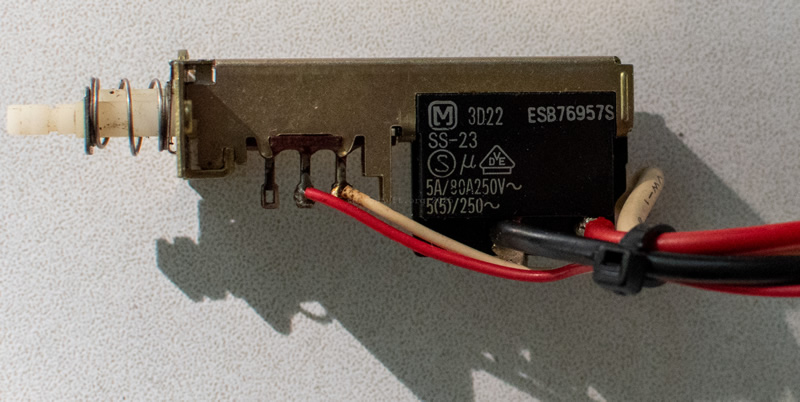
ZR1
TAKAMISAWA
RY5W-K
JAPAN 9348BI
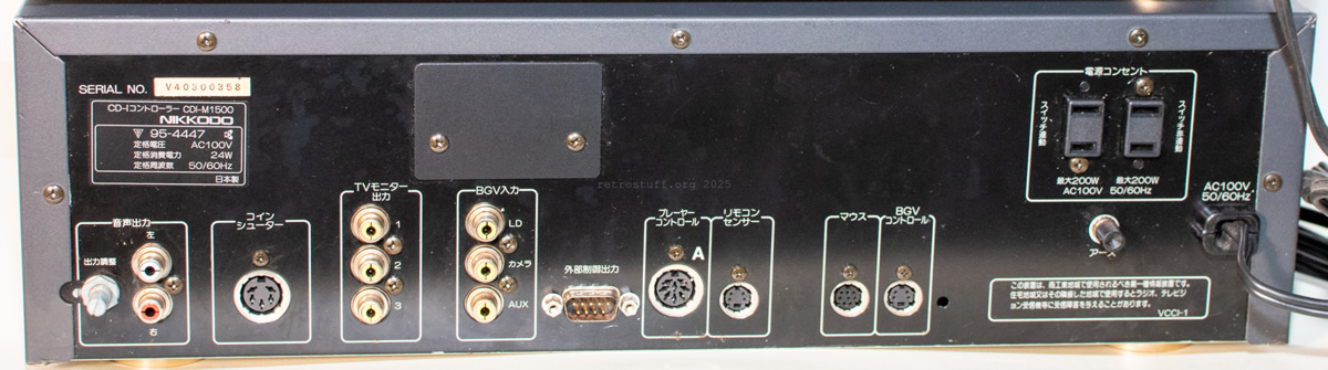
[SIGNAL RELAIS]Back connectors (left to right)
RV1 OUT PUT VOL
YJ1 red/white RCA
CN30 DIN-5
YJ2 yellow/yellow/black RCA
YJ3 yellow/yellow/yellow RCA
CN12 DE-9
CN13 DIN-8
CN14 Mini-DIN-4
CN16 Mini-DIN-8
CN17 Mini-DIN-4
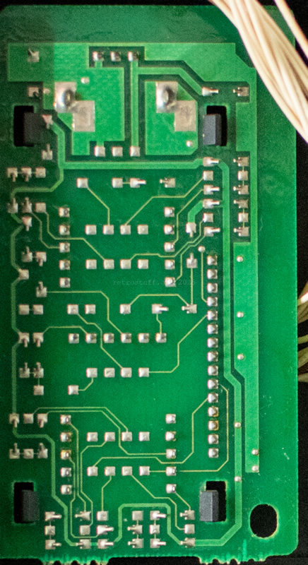
CN18 barrel jackPDCDG4003B (mainboard, back)
U6 (opt. larger footprint U206)
SONY JAPAN
CXK58257AM-10L
339W91YY
[32Kx8 SRAM]
U7 (opt. larger footprint U207)
SONY JAPAN
CXK58257AM-10L
339W91YY
[32Kx8 SRAM]
U14
MN53010KKN
JAPAN 3*N1
U18
(T)9347H
74AC74
[Dual D-Type Positive Edge-Triggered Flip-Flop]
U20
([])3D2T
AC32
[QUADRUPLE 2-INPUT POSITIVE-OR GATES]
U21
(T)9335H
74AC04
[HEX INVERTER]
U25
SONY JAPAN
CXK58257AM-10L
339W91YY
[32Kx8 SRAM]
U28
SONY JAPAN
CXK5864CM-70LL
332M66YY
[8Kx8 SRAM]
U30
SONY JAPAN
CXK5864CM-10LL
327K48YY
[8Kx8 SRAM]
U33
([])2M2T
HC174
[Hex D Flip-Flop with Common Clock and Reset]
U38
([]) 3L1T
HC08
[QUADRUPLE 2-INPUT POSITIVE-AND GATES]
U39
74ACT08
(M)322 JR
[QUAD 2-INPUT AND GATE]
U40
([])2F2T
AC393
[Dual Modulo-16-Counter]
U41
([])3G1T
ACT244
[OCTAL BUFFERS/DRIVERS WITH 3-STATE OUTPUTS]
U42, U43
(Ti)327JLR
HC393
[DUAL 4-BIT BINARY COUNTERS]
U44
(T)9311H
74HCT157A
[Quad 2-input multiplexer]
U45, U46
([])3H2T
HC123A
[Dual retriggerable monostable multivibrator with reset]
U47
(T)9328H
74ACT86
[QUAD EXCLUSIVE OR GATE]
U48
(Ti)310JXS
74LS628
[VOLTAGE-CONTROLLED OSCILLATORS]
U49
4558
3504B
JRC
[DUAL OPERATIONAL AMPLIFIER]
U52
74ACT32
(M)318 DG
[QUAD 2-INPUT OR GATE]
U53
([])3L1T
HC08
[QUADRUPLE 2-INPUT POSITIVE-AND GATES]
U55
([])3G1T
HC125
[QUAD BUS BUFFERS 3-STATE]
U56
([])3L1T
HC00
[Quad 2-Input NAND Gate]
U57
(T)9348H
74HC04A
[Hex Inverter]
U58
(M)277
A521
[Microchip ???]
U59
2229
JRC
A3012B
[SYNCHRONOUS SEPARATION WITH AFC]
U60
(T)9348H
74HC04A
[Hex Inverter]
U61
SONY JAPAN
CXK5864CM-10LL
327K48YY
[8Kx8 SRAM]
U62
([])3M2T
HC30
[8-input NAND gate]
U63
([])3D2T
HC32
[Quad 2-Input OR Gate]
U64
(T)9347H
74AC74
[Dual D-Type Positive Edge-Triggered Flip-Flop]
U65
(T)9342H
74HC07A
[HEX BUFFER OPEN DRAIN]
U66
(M)348
1031
[Video Amplifier Monolithic IC MM1031]
U68
(M)348
1031
[Video Amplifier Monolithic IC MM1031]
U70
4558
3504B
JRC
[DUAL OPERATIONAL AMPLIFIER]
U71
74HC14A
(M) 402JN
[Hex Schmitt-Trigger Inverter High-Performance Silicon-Gate CMOS]
U72
(M)346
60G
[Microchip ???]
U73
(T)9348H
74HC04A
[Hex Inverter]
U74
(T)9347H
74AC74
[Dual D-Type Positive Edge-Triggered Flip-Flop]
U75
(T)9342H
74AC74
[Dual D-Type Positive Edge-Triggered Flip-Flop]
U76
74HCU04
(M)350 NQ
[Hex Unbuffered Inverter]
U77
(M)348
1031
[Video Amplifier Monolithic IC MM1031]
U78
(M)287
A523
[Microchip ???]
U79
(Ti)340JFS
SN7407
[HEX BUFFERS/DRIVERS WITH OPEN-COLLECTOR HIGH-VOLTAGE OUTPUTS]
U80, U81
NE564D
(S)FPA7048
9340VG
[Phase-locked loop]
U82
([])3D2T
HC32
[Quad 2-Input OR Gate]
U83
(T)9348H
74HC04A
[Hex Inverter]
U84
4559
3016A
JRC
[DUAL OPERATIONAL AMPLIFIER]
U85
4559
3016A
JRC
[DUAL OPERATIONAL AMPLIFIER]
U86
74ACT04
(M)329 AY
[HEX INVERTER]
U87
([])3F2T
HCT125
[Quad buffer/line driver; 3-state]
U88
(Ti)332JES
SN75188
[QUADRUPLE LINE DRIVERS]
U89
(Ti)338JJS
SN75189A
[QUADRUPLE LINE RECEIVERS]
U90
74HC14A
(M)402 JN
[Hex Schmitt-Trigger Inverter High-Performance Silicon-Gate CMOS]
U91
([])3G1T
HC125
[QUAD BUS BUFFERS 3-STATE]
U95
4559
3016A
JRC
[DUAL OPERATIONAL AMPLIFIER]
U99
4559
3016A
JRC
[DUAL OPERATIONAL AMPLIFIER]
U102
2249
3002B
JRC
[3-INPUT VIDEO SWITCH]
U104 (unpopulated)
U111
([])3L1T
HC00
[Quad 2-Input NAND Gate]
U113
(M)348
1031
[Video Amplifier Monolithic IC MM1031]
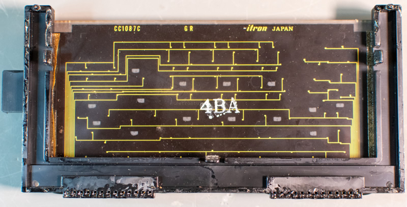
U114 (unpopulated)PDCZR2001A (VFD / button board)
(Don’t mind the condition of the tracks under the VFD, I repaired them later).
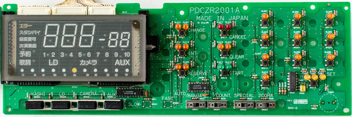
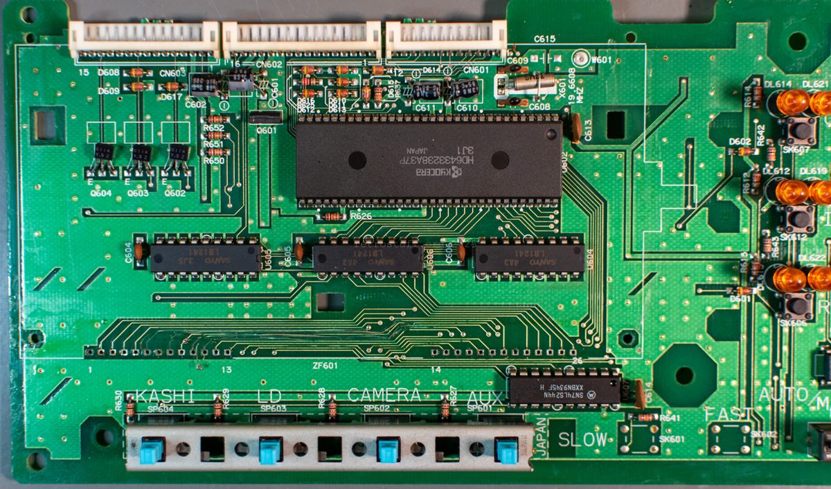
U602
KYOCERA
HD6433238A37P
3J1 JAPAN
[?VFD controller?]
U603
Motorola
SN74LS157N
XJAA9251
[QUAD 2-INPUT MULTIPLEXER]
U604
SANYO 4A3
LB1241
[Fluorescent Display Tube Driver]
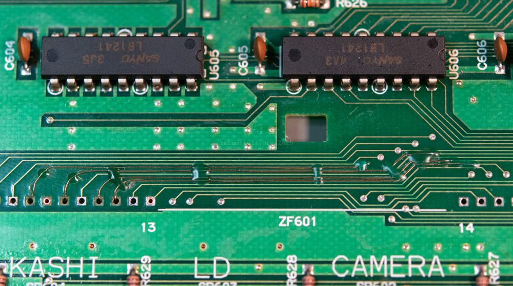
U605
SANYO 3J5
LB1241
[Fluorescent Display Tube Driver]
U606
SANYO 4A3
LB1241
[Fluorescent Display Tube Driver]
U607
Motorola
SN74LS244N
XXBN9345F H
[OCTAL BUFFER/LINE DRIVERWITH 3-STATE OUTPUTS]
U608
Motorola
MC74HCU04N
JJAB9404B
[Hex Unbuffered Inverter]
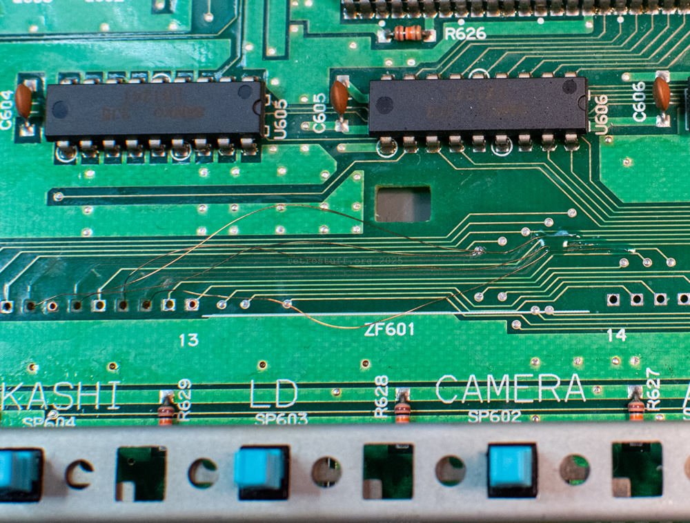
ZF601
[VFD]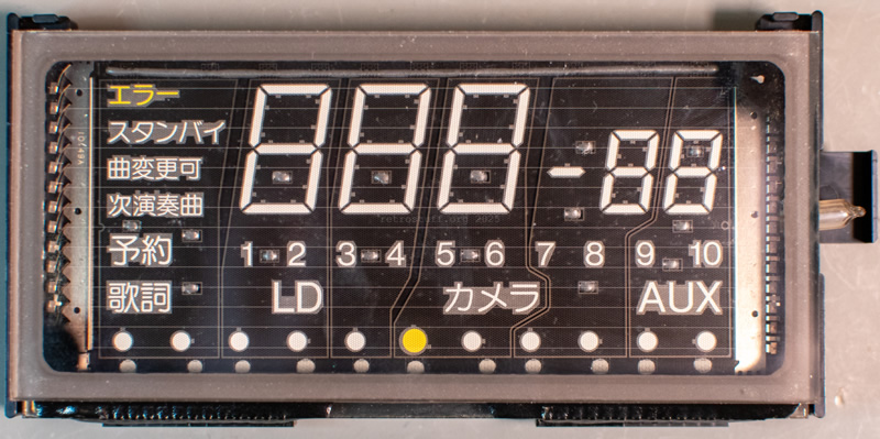
Connectors
CN601 12 pin -> mainboard CN3
CN602 16 pin -> mainboard CN2
CN603 15 pin -> IR board CN901
Switches and buttons
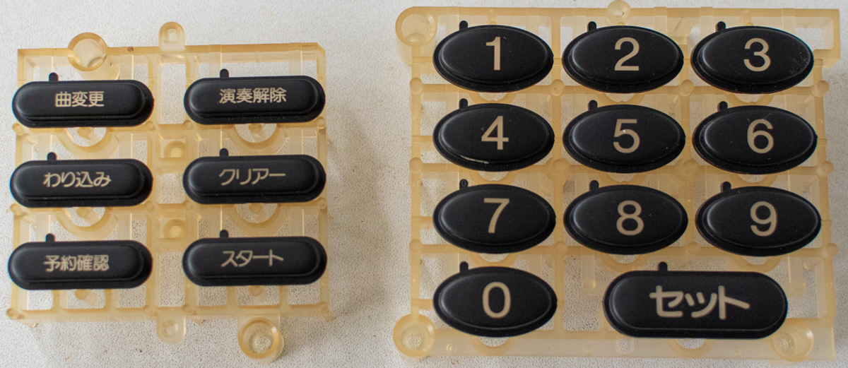
Bottom row (left to right):
SW605
- SP604 KASHI
- SP603 LD
- SP602 CAMERA
- SP601 AUX
SK601 SLOW (unpopulated)
SK602 FAST (unpopulated)
SW601 AUTO/MANUA
SW604 1/COUNT
SW602 SPECIAL
SW603 2CORA
Middle block:
SK607 CHANGE SK617 CANCEL
SK612 INT SK611 CLEAR
SK606 RESERVE SK616 START
Number block:
SK603 1 SK608 2 SK613 3
SK618 4 SK604 5 SK609 6
SK614 7 SK619 8 SK605 9
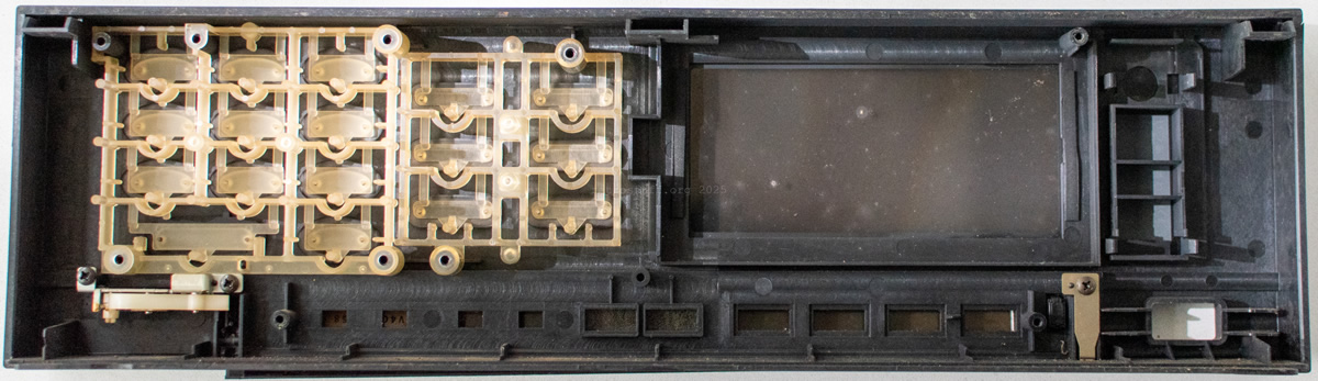
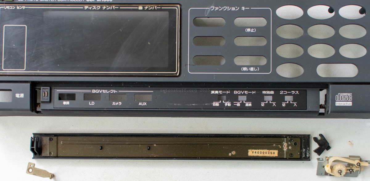
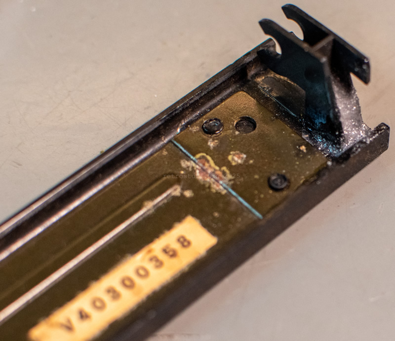
SK610 0 SK615 SETPDLDR2001A (Traffic light / IR board)
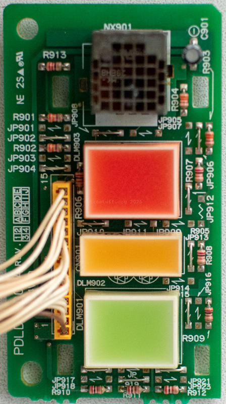
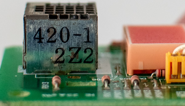
CN901 soldered connector 15 pin -> VFD board CN603
NX901
IR cage 420-1 | 2Z2
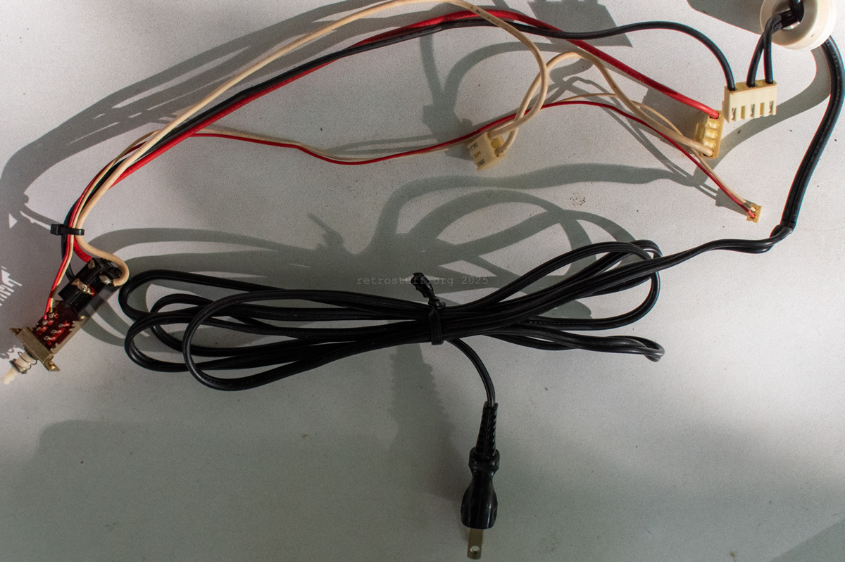
Tiny sub PCB inside: CMK-29EHBPDZZR2001A (Power connector board)
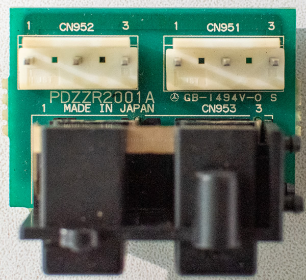
CN951 3 pin -> power cable, power switch
CN952 3 pin -> power switch, PSU CN1
PSU Nichicon CI-1PS
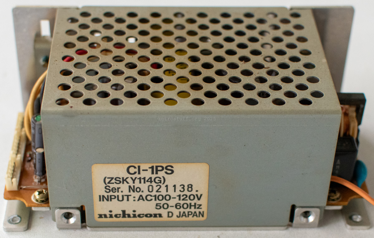
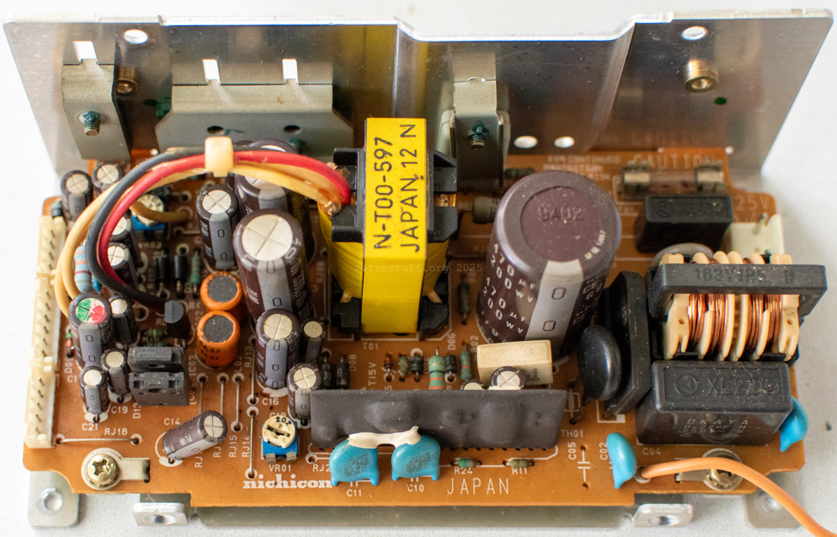
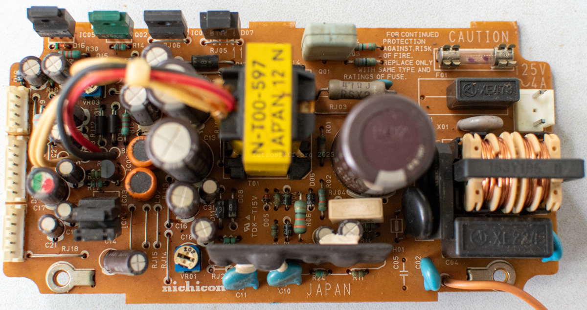
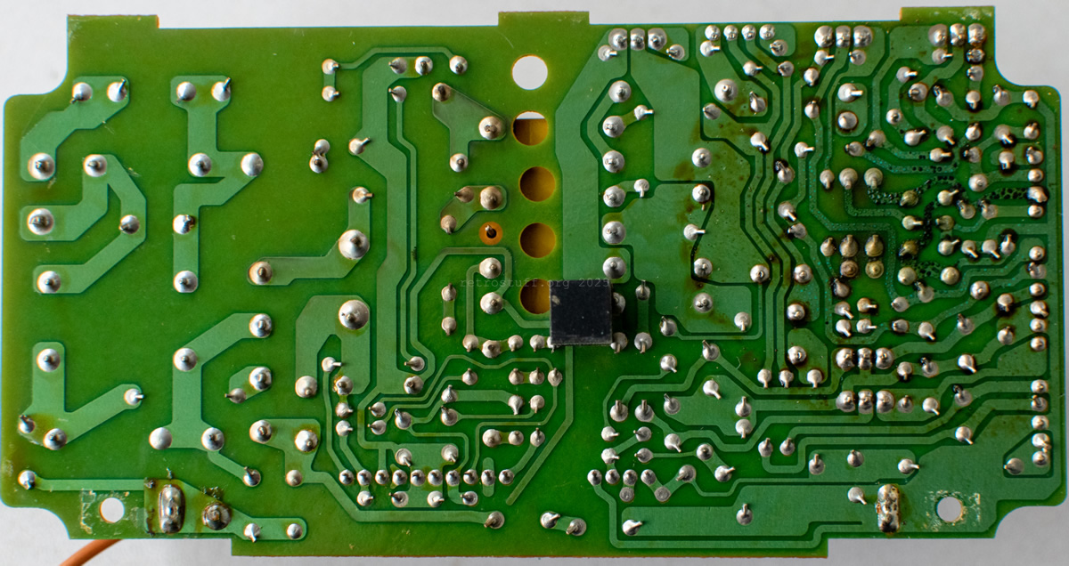
CI-1PS
(ZSKY114G)
Ser. No. 021138.
INPUT:AC100-120V
50-60Hz
nichicon D JAPAN
The power supply only came on once and then went off for good. I had done all the other tests on the V unit using the power supply from the A unit (before I took it apart).
To-do
There is still a long way to go to rebuild the PSU. Here are some photos of the progress of cleaning and sanding the PCB and riveting some through holes:
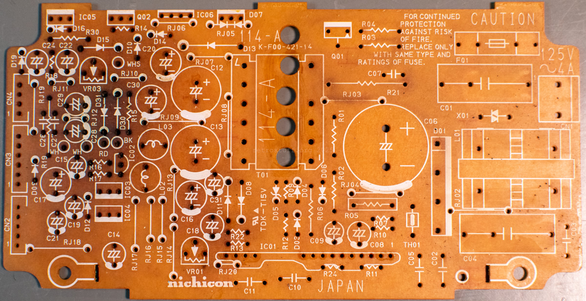
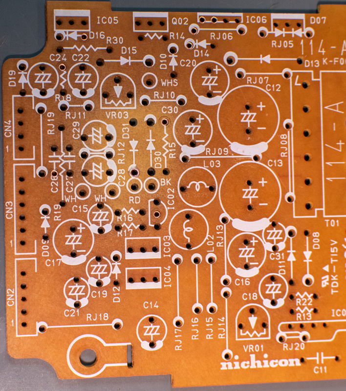
Components
| ID | Marking | Measured |
|---|---|---|
| C01 | 0,047 / 250 / XE473 | 0.047uF M | 250V~ :5 | (M?) (OeVE) | 45,04nF |
| C02 | 1nF / 250/400 / KC102K | 1,006nF |
| C03 | 1nF / 250/400 / KC102K | 1,001nF |
| C04 | XE224 | OKAYA | 0,22uF M | 250V~ .6 | (M?)(OeVE) | 200,8nF |
| C05 | (not populated) | |
| C06 | 470 / 200W / nichicon | CE 105oC | GC (M) | 9402 | 444,8 0,06R |
| C07 | HR | 22IJ | IKV | 226,6pF |
| C08 | 47 / 50 / nichicon | PL (M) | 105°C | H9350 | 46,24 0,26R |
| C09 | 0,47 / 50 / nichicon | PF (M) | 105°C | H9353 | 0,48 5,9R |
| C10 | 0,0022 / 250/400 / KC222M | 2,116nF |
| C11 | 0,0022 / 250/400 / KC222M | 2,161nF |
| C12 | 3300 / 10 / nichicon | PL (M) | 105°C | H9345 | 3412 0,03R |
| C13 | 3300 / 10 / nichicon | PL (M) | 105°C | H9345 | 3424 0,03R |
| C14 | 100 / 25 / nichicon | PL (M) | 105°C | H9351 | 108,7 0,27 |
| C15 | 33 / 25 / nichicon | PF (M) | 105°C | H9347 | ICL |
| C16 | 330 / 25 / nichicon | PL (M) | 105°C | H9350 | 286,6 0,11R |
| C17 | 330 / 25 / nichicon | PL (M) | 105°C | H9350 | 288,8 0,09 |
| C18 | 100 / 25 / nichicon | PL (M) | 105°C | H9351 | 107,0 0,27R |
| C19 | 33 / 25 / nichicon | PF (M) | 105°C | H9347 | 30,44 6,4 |
| C20 | 330 / 25 / nichicon | PL (M) | 105°C | H9350 | 290,2 0,10R |
| C21 | 33 / 25 / nichicon | PF (M) | 105°C | H9347 | 31,58 4,3 |
| C22 | 47 / 50 / nichicon | PL (M) | 105°C | H9350 | 46,26 0,24 |
| C24 | 47 / 35 / nichicon | PF (M) | 105°C | H9350 | 45,47 0,69 |
| C26 | 104K | |
| C27 | 104K | |
| C28 | 100 / 25 / nichicon | PL (M) | 105°C | H9351 | ICL |
| C29 | 100 / 25 / nichicon | PL (M) | 105°C | H9351 | nm >40 |
| C30 | 680 / 10 / nichicon | PF (M) | 105°C | H9346 | 701,0 0,13R |
| C31 | 0,47 / 50 / nichicon | PF (M) | 105°C | H9353 | 0,47 7,1R |
| CN1 | (2pin) | |
| CN2 | (5pin) | |
| CN3 | (6pin) | |
| CN4 | (4pin) | |
| D01 | (->||<-) D3SB 40 3D | |
| D03 | 02 | 3N | 0,541V@5,00mA |
| D04 | 02 | 3N | 0,542V@5,00mA |
| D05 | 272 | 0,770V@5,00mA |
| D06 | 02 | 3O | 0,544V@5,00mA |
| D07 | 3D | C85M | ->||<- | 009 | 0,205V@5,00mA |
| D08 | B91 | 02 | 39 | 0,522V@5,00mA |
| D09 | (glass) | 0,683V@5,00mA |
| D10 | 02 | 38 | 0,700V@5,00A |
| D11 | B91 | 02 | 3N | 0,516V@5,00mA |
| D12 | (glass) | 0,683V@5,00mA |
| D13 | B93 | 02 | 38 | 0,485V@5,00mA |
| D14 | (glass) | 0,680V@5,00mA |
| D15 | 41B3806 | 0,517V@5,00mA |
| D16 | (glass) | 0,683V@5,00mA |
| D19 | 02?? | 0,666V@5,00mA |
| D30 | ??? | 0,520V@5,00mA |
| D31 | ??? | 0,522V@5,00mA |
| F01 | (T)(A) 125V4A | SOCTSC | |
| IC01 | MA5333 | .3Y2 | |
| IC02 | M5237L | 3804 | ? |
| IC03 | NEC JAPAN | 24M09 | 9301E | |
| IC04 | 79M09A | JRC | M2013F | ? |
| IC05 | NEC JAPAN | 79M24 | 9231F | |
| IC06 | PQ05RF2 | SHARP | E1 | |
| L01 | 163Y1R5 N | 25,25mH 25,23mH |
| L02 | RD810A3F | 3 µH | 2,96µH |
| L03 | RD810A3F | 3 µH | 3,01µH |
| Q01 | T | K1118 | 4A | MOSFET |
| Q02 | .T | B1015 | Y ?3K | |
| R01 | 68,3k | |
| R02 | 68,2k | |
| R03 | 26,90R | |
| R04 | 9,762k | |
| R05 | RGC2 | 0.15OJ | NOBLE U30 | 0,18R |
| R06 | 33,09R | |
| R07 | 91,36R | |
| R09 | 67,3~5k | |
| R10 | 11,97k | |
| R11 | 3,312k | |
| R12 | 100,1R | |
| R13 | 3,945k | |
| R14 | 221,3R | |
| R15 | 119,7R | |
| R16 | 3,919k | |
| R17 | 994,3R | |
| R18 | 560R | |
| R19 | 3,267k | |
| R21 | 47OJ | RSX2 | 47OJ | FD?-3 NY | 47OJ | 48,51R |
| R22 | 69,00R | |
| R24 | 56,50k | |
| R30 | 3,270k | |
| RJ02 | (wire) | |
| RJ03 | (wire) | |
| RJ04 | (wire) | |
| RJ05 | (wire) | |
| RJ06 | (wire) | |
| RJ07 | (wire) | |
| RJ08 | (wire) | |
| RJ09 | (wire) | |
| RJ10 | (wire) | |
| RJ11 | (wire) | |
| RJ12 | (wire) | |
| RJ13 | (wire) | |
| RJ14 | (wire) | |
| RJ15 | (wire) | |
| RJ16 | (wire) | |
| RJ17 | (wire) | |
| RJ18 | (wire) | |
| RJ19 | (wire) | |
| RJ20 | (not populated) | |
| T01 | N-T00-597 | JAPAN 12 N | |
| TH01 | (S) (ca?) | 8D-13 | HR | |
| VR01 | 202 | |
| VR03 | 103 | |
| X01 | (EE) 3D | ENC271 | 618,pF |
Repairs done
Overview of what’s been done so far (apart from cleaning the whole unit and especially the mainboard from insects and dirt).
First, random impressions of everything except the PCBs while disassembling and cleaning everything:
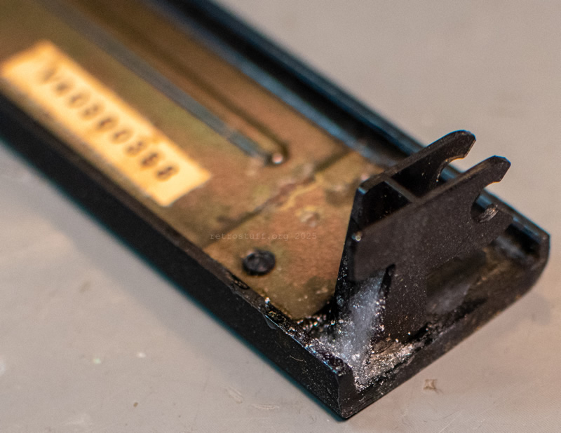
Front panel
Disassembling and cleaning the entire front panel. The right hinge of the flap was broken, so I fixed it with a mixture of superglue and baking soda. Let’s see how long it lasts.

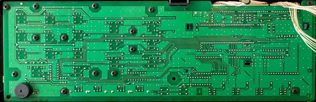
VFD / button board
The VFD / button board (PDCZR2001A) was damaged when I removed the VFD: it was soldered on both sides without me noticing, taking a couple of eyelets and four tracks with it.
I repaired it with enamelled copper wire, green UV solder mask and 0,6 mm rivets. The rivets were a bit short, but it all worked out in the end.


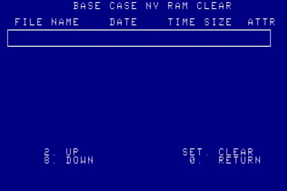
Battery
The battery that backs up the NVRAM and RTC was of course empty (date code 93-12) and I replaced it with a new CR17335SE (2/3A) lithium cell. I used a normal clear heat shrink tube that shrinks at about 90 °C or higher – which was quite a gamble and took a lot of time to shrink properly.
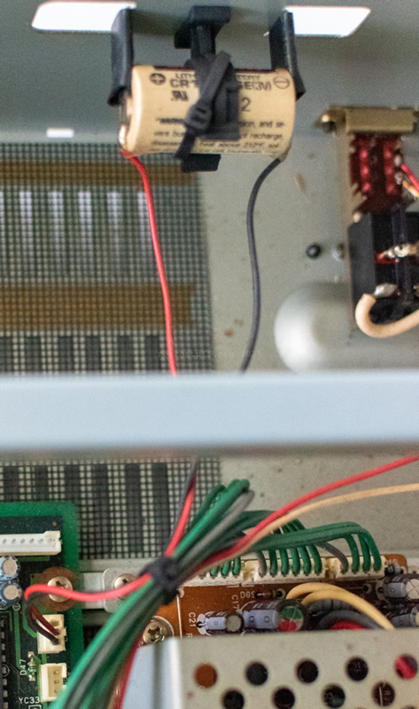

I later bought a special PCV shrink tube for batteries, which shrinks at about 80°C, to give me more peace of mind for the other units.
Credits
Many thanks to
– CD-i Fan for creating the first draft of the chip marking list and analysing the system ROM
– ogarvey for converting stx.dyuv
History
2025-02-23: Initial WIP Page published
2025-06-14: System ROM information added